
In applications such as communications power supplies, motor drives, and Class D audio power amplifiers, hard-switching topologies must deal with a thorny problem—the reverse recovery charge (Qrr) of the power MOSFET body diode. If Qrr is too high, at best system efficiency drops sharply and heating worsens; at worst it triggers uncontrolled ringing at the switching node and voltage overshoot, forcing engineers to add extra snubber circuits, putting both cost and space under pressure.
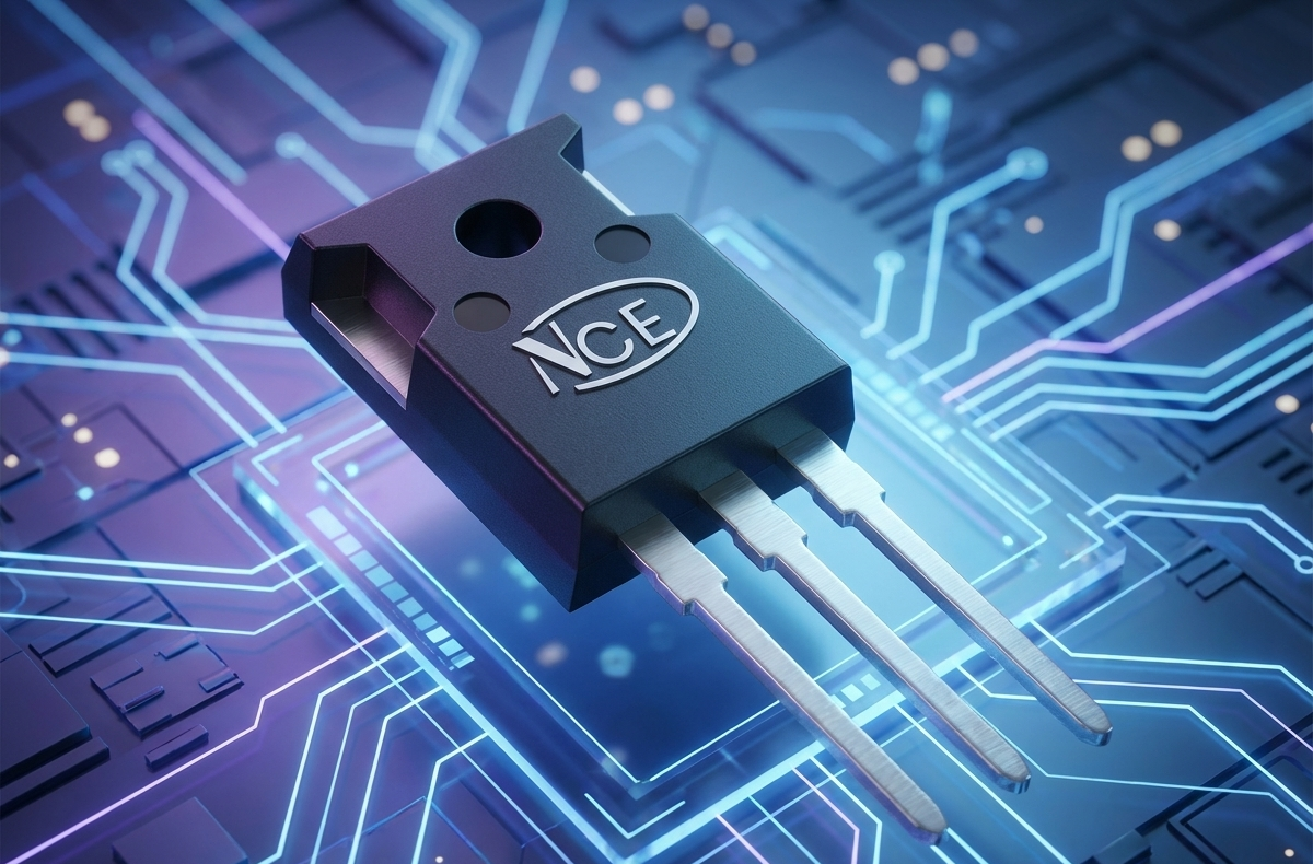
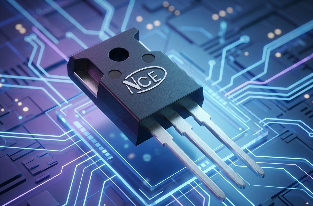
The newly launched 250V SGT (shielded gate trench) power MOSFET NCEP025S90T from Wuxi NCE Power debuts as part of the "Super Recovery" ultra-fast recovery series. With low reverse recovery charge, it offers a better choice for hard-switching applications requiring high performance and high reliability.
1. Qrr—The Performance Bottleneck of Hard-Switching Topologies
The body diode of a power MOSFET is naturally formed by the PN junction inside the device and is an inherent parasitic diode structure in the manufacturing process. While it provides freewheeling and protection functions in the circuit, it also introduces additional losses and design challenges.
When the device is in forward conduction, a large number of minority carriers are injected and stored inside the PN junction. Once the device needs to switch from forward conduction to reverse blocking, these stored carriers must first be "swept out" before the body diode can recover its blocking capability; this process is called reverse recovery. The reverse recovery charge Qrr is precisely the core parameter defining the total amount of carriers in this process—the total charge enclosed by the entire reverse recovery waveform from the current zero crossing until the reverse recovery current decays to a specified value. This parameter is directly related to a difficult engineering problem in hard-switching systems—reverse recovery loss and voltage overshoot.
In a typical hard-switched bridge circuit, the Qrr stored when the low-side body diode freewheels is forcibly extracted at the instant the high-side switch turns on, causing an additional spike pulse in the high-side turn-on current. This not only increases the instantaneous stress on the switching device but also excites severe voltage ringing and overshoot on parasitic inductance, directly threatening system reliability. In short, the larger Qrr is, the higher the loss, the more severe the overshoot, the harder EMI is to suppress, and the more complex the snubber circuit design becomes.
II. Targeted Optimization of SGT Technology: Reverse Recovery Charge (Qrr) Reduced by 86%
Based on SGT shielded-gate trench technology, NCE Power has carried out targeted optimization of the reverse recovery characteristics of the MOSFET body diode. The reverse recovery charge of the ultra-fast reverse recovery product NCEP025S90T is reduced by 86% compared with the previous-generation product.
The drift region of a conventional trench MOSFET exhibits a triangular distribution, whereas the SGT structure, by introducing a shielded gate, superimposes a horizontal depletion effect on the vertical depletion of a conventional trench MOSFET, shaping the electric field in the drift region into an approximately rectangular distribution. This change effectively reduces the drift-region resistance at the same breakdown voltage while optimizing the switching characteristics of the body diode, thereby reducing reverse recovery charge and shortening reverse recovery time.
To quantitatively evaluate the optimization effect, NCE Power compared the body-diode reverse recovery performance of NCEP025S90T with that of the previous-generation general-platform product NCEP02590T on a double-pulse test platform. The test conditions were: forward current IF = 45 A and current change rate di/dt = 100 A/μs. The results are as follows:
- Reverse recovery time (Trr): shortened from 163 ns to 67 ns, a reduction of 58.9%;
- Reverse recovery charge (Qrr): reduced from 1307 nC to 178 nC, a reduction of 86%;
- Peak reverse recovery current (Irrm): reduced from 16 A to 5 A.

Reverse recovery comparison test waveforms of NCEP02590T (left) and NCEP025S90T (right) (source: official)
The 86% reduction in Qrr is by no means merely an on-paper numerical optimization; it translates directly into three clear engineering benefits:
1. Effective suppression of overshoot voltage. Reverse recovery charge is the energy source of ringing at the switching node; with a substantial reduction in Qrr, the VDS spike naturally decreases. Snubber circuit parameters no longer need excessive redundancy for worst-case conditions; the RCD snubber network can even be simplified, benefiting both BOM cost and PCB area.
2. Significantly lower switching loss. For every bit that Qrr is reduced, the excess charge drawn during the reverse recovery period of the freewheeling diode is reduced accordingly, and the current surge that the main switch must withstand at turn-on is weakened. This is especially critical for efficiency improvement under the trend toward higher frequencies.
3. Greatly improved EMI friendliness. Ringing amplitude and harmonic components are reduced simultaneously, mitigating the sources of conducted and radiated interference and easing filter design pressure.
III. RRSOA improved by more than 5 times, reinforcing the safety margin
In inductive-load applications such as motor drives and inverter circuits, the MOSFET body diode must not only turn off, but turn off reliably. The reverse recovery safe operating area (RRSOA) is a key hard metric for evaluating the body diode's dynamic freewheeling withstand capability—it determines whether the device will enter dynamic avalanche failure when subjected to high di/dt and reverse voltage stress.
NCE Power conducted progressively stricter double-pulse stress tests on NCEP025S90T and the previous-generation product NCEP02590T: the experiment used a double-pulse circuit, with the switching transistor (Q1) and freewheeling transistor (Q2) each replaced by the device under test at the same time; the pulse width was increased step by step to raise the freewheeling transistor current, and the pass condition of the freewheeling transistor during the reverse recovery phase was recorded.

Double-pulse test circuit diagram (image source: official)

Photo of the double-pulse test platform (image source: official)
Test results show that the reverse recovery safe operating area (RRSOA) of the NCEP025S90T is more than 5× better than that of the previous-generation product, with no significant degradation of RRSOA at high temperature and excellent high-temperature dynamic reliability of the body diode. This means that under harsh conditions such as frequent motor braking, commutation, or bridge-leg shoot-through freewheeling, the device's body diode has a wider safety margin and will not easily become the weak link in the system. For designs such as 48 V–100 V power tools, drone ESCs, and servo drives, this feature provides considerable peace of mind.
RRSOA comparison test results
| Product | Temperature (°C) | VDD(V) | Vgs(V) | ISD(A) | Test results |
| NCEP02590T | 25 | 200 | 20 | 57 | PASS |
| 67 | NG | ||||
| 125 | 200 | 20 | 11 | PASS | |
| 20 | NG | ||||
| NCEP025S90T | 25 | 200 | 20 | 335 | PASS |
| 125 | 200 | 20 | 335 | PASS |
Note: 335 A in the table is the upper limit of the equipment's current capability, not the overcurrent capability limit of the MOSFET.
IV. Electrical parameters are highly compatible, supporting design upgrades
To help engineers achieve product upgrades at minimal cost, the NCEP025S90T maintains high consistency with the previous-generation product NCEP02590T in the remaining dynamic and static electrical parameters and uses the same package (TO-247), so the original design can be compatibly replaced with almost no adjustment. The specific parameter comparison is as follows:
| Key Parameters | Conditions | NCEP025S90T | NCEP02590T |
| Breakdown Voltage (Bv) | Ids=250uA | 282V | 282V |
| Threshold Voltage (Vth) | Ids=250uA | 3.42V | 3.44V |
| Input Capacitance (Ciss) | Vds=50%BV,Freq=1MHZ | 6100pF | 6050pF |
| Output Capacitance (Coss) | 340pF | 330pF | |
| Gate Charge (Qg) | Id=20A,Ig=0.2mA | 103nC | 105nC |
| On-resistance (Ron) | Vgs=10V,Id=20A | 18.60mΩ | 14.90mΩ |
As can be seen from the table, the device's input capacitance Ciss and gate charge Qg fluctuate only slightly, so the drive circuit basically requires no adjustment, and the existing design can be directly replaced. The only trade-off is on-resistance: Ron changes from 14.90 mΩ to 18.60 mΩ.
However, note that in the vast majority of hard-switching applications, the system-level benefit from reduced switching losses will far outweigh the slight temperature-rise penalty of this less-than-4 mΩ increase in on-resistance, especially as switching frequencies move toward the hundreds of kHz range; the balance of the efficiency curve will tilt toward NCEP025S90T.

Naming convention (image source: official)
V. Application Scenarios
With the core advantages of low reverse recovery charge and a wide reverse recovery safe operating area (RRSOA), NCEP025S90T can be used in:
- 48V–100V motor control systems: power tools, low-voltage servo drives, robot joints, drone ESCs, etc.; the wide RRSOA provides reliable protection for frequent motor commutation and braking;
- Communication power supplies: 48V bus DC-DC converters, ideal as a primary-side switch or secondary-side synchronous rectifier; low Qrr helps power supplies achieve higher frequency and higher power density.
- Industrial Power Supplies and Inverter Circuits: For scenarios such as high-power-density industrial power modules and compact inverters that impose stringent requirements on efficiency and reliability, it simplifies EMI and snubber circuit design and improves long-term system stability;
- Class-D Audio Amplifiers: The low Qrr characteristic reduces switching distortion, lowers the audio noise floor and distortion, and improves sound purity and the listening experience.
6. Conclusion
NCEPOWER NCEP025S90T is a power device that reasonably sacrifices a small amount of on-resistance performance in exchange for a revolutionary improvement in body-diode reverse-recovery performance. Its low Qrr effectively suppresses voltage spikes and simplifies EMI filter design; the wide RRSOA ensures stable operation under extreme system conditions, making it particularly suitable for hard-switching topologies that require high switching frequency or freewheeling with inductive motor loads.For more information about NCEPOWER products or to request samples, please contact the official authorized distributor: sales@chiplinkstech.com; contact phone: Mr. Chen, 13924675549 (same number on WeChat); WeChat Official Account: Zhilian Micro - Motor Control Chips, providing product selection services and technical support.

Attached: Sample Request

WeChat Official Account