
In midsummer 2026, the global semiconductor industry entered a new wave of widespread price increases. More than 20 semiconductor companies worldwide, including Texas Instruments, Infineon, and STMicroelectronics, began implementing the second round of 2026 price increases on July 1, raising power chip prices by 15% to 25%; among them, scarce power devices related to AI servers posted the largest gains, with some core models rising more than 50% cumulatively during the year. A person at a power semiconductor manufacturer said bluntly: 'Our AI-related power orders are completely full; we simply cannot keep up with orders now.'
Orders are overflowing and prices are jumping—all of this stems from the exponential growth in power consumption of AI computing clusters.
1. Power Consumption Soars: AI Servers Are 'Eating' More and More Electricity
In 2026, the power consumption curve of AI servers is growing explosively. The single-chip power consumption of NVIDIA's new-generation Rubin GPU has been locked at 2.3 kW. According to industry estimates, a Vera Rubin NVL72 rack consumes up to 230 kW—roughly equivalent to 140 household air conditioners running at full power simultaneously. In the Rubin Ultra generation, per-rack power consumption will soar to 660 kW.
Surging power consumption brings a multiplied increase in current demand. According to Sigmaintell Consulting, global AI server shipments will reach about 3.7 million units in 2026, up 51.3% year on year. TechInsights forecasts that data center power semiconductor revenue will reach US$5 billion in 2026 and grow to US$14.3 billion by 2031. onsemi expects that the AI data center-related TAM will reach US$12.2 billion by 2029, with a CAGR of about 40%.
At present, the semiconductor value per kilowatt in AI server power supplies has risen to about US$175. As the penetration rate of third-generation semiconductor power devices increases, the value per kilowatt will continue to climb.
II. From the Power Grid to the GPU Core: A “Six-Stage Relay”
The power supply of an AI server does not simply deliver AC power to the GPU. From the power grid to the GPU core, electrical energy must undergo multiple stages of conversion—each stage requires specific power devices.
According to mainstream industry designs, AI server power supply units (PSUs) typically use a two-stage “PFC + LLC” architecture. The entire power delivery chain can be divided into six key nodes:
| Node | Function | Key Device Requirements |
| ①PFC | 220 V/380 V AC → 400 V DC bus | 650 V superjunction MOSFET, low on-resistance, optimized body-diode reverse recovery |
| ② LLC primary side | 400V DC → high-frequency AC | 650V superjunction MOSFET, low Qrr/Trr, suitable for soft switching |
| ③ LLC secondary side | Low-voltage AC → 48V/12V DC | 60V-85V SGT MOSFET, ultra-low on-resistance |
| ④48V ORing | Multi-rail power redundancy management | 60V-85V SGT MOSFET, low on-resistance |
| ⑤48V→12V IBC | Bus voltage step-down | 60V-85V SGT MOSFETs with low switching loss |
| ⑥VRM | 12V/48V→<1V GPU core power supply | 30V-40V SGT MOSFETs with ultra-low on-resistance in small packages |
These six nodes may seem numerous, but their requirements for power devices can be summarized into three major technology segments: the high-voltage AC/DC side (nodes ①②), the low-voltage DC/DC side (nodes ③④⑤), and the core power supply VRM (node ⑥).
In addition, hot-swap protection circuits and auxiliary power supplies are also indispensable components. Around these segments, NCE Power has built a complete power device matrix for AI server power supplies.
III. Three Core Segments: A “Product Map” Covering the Full Chain
In the fast-growing AI server power supply market, NCE Power has established four product process platforms: IGBT, shielded-gate MOSFET (SGT MOSFET), super-junction MOSFET (SJ MOSFET), and trench MOSFET (Trench MOSFET). It has successively launched automotive-grade power devices, SiC MOSFETs, GaN HEMTs, power modules, IPM intelligent power modules, and other products. It currently offers more than 4,000 product models, covering a full voltage range of 12V–1700V, and can be widely used in key stages such as power supply units, voltage regulator modules, HVDC systems, and SSTs for AI servers and data centers. Related products have entered the mass supply stage with many domestic and overseas customers.
The following sections elaborate on the three core blocks one by one. In addition, although hot-swap protection and auxiliary power are not part of the main power chain, they are also critical to reliable system operation and are introduced as supplementary content in this article.
Block 1: High-Voltage AC/DC Side — PFC and LLC Primary Side
This is the highest-voltage stage in the entire chain and the first gate that determines the power factor and energy-efficiency rating of the whole system.
At the two high-voltage nodes—PFC boost and LLC primary-side switching—engineers face a core trade-off: how to pursue lower on-resistance (Rds(on)) while also accounting for the additional losses caused by body-diode reverse recovery. In a boost PFC topology, the main switch operates in hard switching, and the key to device selection is achieving the optimal balance between conduction loss and switching loss. In continuous conduction mode (CCM) PFC, conventional superjunction MOSFETs have excessive body-diode reverse-recovery charge (Qrr), resulting in significant switching losses and EMI issues. In LLC resonant topologies, if the body-diode reverse-recovery time (Trr) is not short enough, ringing spikes occur, forcing designers to add snubber circuits and sacrificing efficiency and space.
NCE Power has positioned two major product platforms in this block, SJ-III TF and SJ-IV NF, covering different power levels and application scenarios.
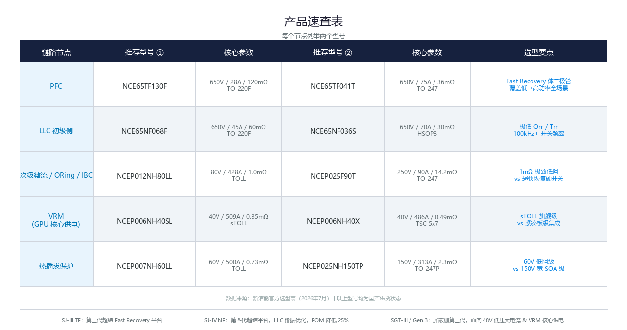
The SJ-III TF series is based on the third-generation superjunction technology platform. For switching applications such as full-bridge, half-bridge, and LLC, it enhances the body-diode reverse-recovery characteristics. Take NCE65TF130F (650 V/28 A/120 mΩ/TO-220F) as an example: its body diode features Fast Recovery, which effectively suppresses the additional losses and voltage spikes caused by reverse recovery in CCM PFC circuits, allowing designers to pass EMI testing without adding an extra RC snubber. The series also offers models with higher current ratings, covering PFC scenarios from low power to high power.
The SJ-IV NF series is optimized specifically for LLC resonant converters. It uses the fourth-generation superjunction technology platform and, while ensuring industry-leading ultra-low on-resistance, focuses optimization on body-diode characteristics, greatly reducing reverse-recovery charge (Qrr) and reverse-recovery time (Trr), thereby significantly lowering reverse-recovery losses in bridge circuits such as LLC. Compared with the previous generation, Rds(on) is reduced by 16%, the figure of merit (FOM) is reduced by 25%, and gate charge is significantly lower. It supports switching frequencies above 100 kHz—meaning engineers can raise the switching frequency from the common 65 kHz to above 100 kHz without sacrificing efficiency, thereby reducing transformer and inductor size and improving overall power density.
Take NCE65NF068F (650 V/45 A/60 mΩ/TO-220F) as an example: it achieves 60 mΩ on-resistance and 65 nC gate charge in a fully molded insulated package. Its built-in fast-recovery body diode shortens reverse-recovery time to the 150 ns level, effectively suppressing reverse-recovery spikes in LLC resonant circuits and eliminating the need for an external snubber. The TO-220F package eliminates the external insulating pad, simplifying assembly while improving safety and reliability—for mass production, this means lower assembly cost and higher first-pass yield.
The SJ-IV series also offers automotive-grade versions (AEC-Q101 certified), covering a breakdown voltage range of 500V to 1050V. For example, the NCEA65NF068D7 (650V/60mΩ/45A/TO-263-7L) has a gate charge of 65nC, single-pulse avalanche energy (EAS) up to 360mJ, and maximum power dissipation of 371W—capable of easily handling voltage spikes caused by lightning strikes or load transients in PFC circuits, providing ample margin for system reliability.
For high-power-density PSUs above 800W, the SJ-IV NF series offers an even more extreme choice. The NCE65NF036S (30mΩ/70A) can further reduce conduction losses, making it an advanced choice for high-density PFC and LLC primary sides.
Section 2: Low-voltage DC/DC Side—LLC Secondary Synchronous Rectification and 48V Bus
Having covered the high-voltage side, let's now look at the low-voltage high-current side.
In the three nodes of LLC secondary synchronous rectification, 48V ORing redundant management, and 48V→12V IBC conversion, engineers face a highly consistent core challenge: how to minimize conduction losses under high currents ranging from tens to hundreds of amperes, while solving thermal issues within limited board space. For every 1W increase in losses at these three nodes, the entire PSU's cooling system requires approximately 3W of additional cooling power—an unacceptable trade-off in AI servers where power density continues to climb.
NCE Power's SGT MOSFET product line has achieved complete coverage from 60V to 250V in this segment.
At the two nodes of secondary synchronous rectification and 48V ORing, the flagship model of the SGT-III series, NCEP012NH80LL (80V/428A/1.0mΩ/TOLL), with an on-resistance of only 1.0mΩ, reduces conduction losses under high currents to the milliwatt level. This model can simultaneously meet the requirements of the three major nodes: secondary rectification, ORing, and IBC. A single part number unifies the BOM, reducing supply chain complexity; its single-device current capability of 428A and extremely low resistance of 1.0mΩ enable a current handling level that previously required 2-3 devices in parallel to be achieved with just one device, simplifying board layout. Compared with traditional TO-220/TO-247, the TOLL package significantly improves the thermal path and parasitic inductance, making it particularly suitable for high-density, high-current 48V bus applications. Among these, the IBC stage, due to its higher operating frequency, also has certain requirements for switching losses—the low Qg design of NCEP012NH80LL allows it to maintain low switching losses even at high frequencies.
To address the efficiency challenges caused by body diode reverse recovery in hard-switching topologies, NCE Power has introduced the 250V ultra-fast recovery SGT MOSFET NCEP025S90T. Its reverse recovery charge (Qrr) is reduced by 86% compared to the previous generation, and the reverse recovery time is shortened from 163ns to 67ns. This characteristic is particularly critical during the conduction period of the body diode in the synchronous rectifier of secondary rectification—shorter recovery time means lower switching losses and cleaner switching waveforms, directly improving overall system efficiency.
Section 3: GPU Core Power Supply (VRM)—The Most Demanding Link in the Entire Chain
VRM is the link in the entire AI server power chain that places the highest requirements on power devices. GPU core voltages have dropped below 1V, while currents reach hundreds of amperes—this means power devices must achieve extremely low on-resistance and very high switching frequency at very low voltage.
The core contradiction in this link is how to fit dozens of parallel power phases into board-level space the size of a fingernail while ensuring that the losses of each phase are low enough to make the thermal solution feasible. If the on-resistance of each VRM phase is 1 mΩ higher, at currents of hundreds of amperes, the additional heat dissipation may cause the temperature of the entire power module to exceed specifications.
NCE Power's SGT-III Gen.3 series is tailored specifically for this scenario. This series uses internationally advanced shielded-gate trench process technology. Compared with SGT-II, specific on-resistance (Ron·sp) is reduced by 33%, and figure of merit (FOM) is reduced by 31%. The flagship model NCEP006NH40SL (40V/509A/0.35mΩ/sTOLL) represents the very high level of NCE Power's SGT process—0.35mΩ on-resistance means that at 500A current, conduction loss is only 87.5W, an highly attractive figure for VRM thermal design. The sTOLL package further optimizes the thermal path and package internal resistance based on TOLL, providing ample design margin for next-generation GPU VRM multiphase parallel architectures.
On the board-level integrated DFN/TSC package route, NCEP006NH40X (40V/486A/0.49mΩ/TSC5×7) achieves near-TOLL-level performance in a compact 5mm×7mm package, making it suitable for high-density multiphase VRM layouts; on the TOLL package route, NCEP005NH40LL (40V/800A/0.43mΩ/TOLL) provides a more ample thermal path with 800A current capability, making it suitable for scenarios with higher thermal management requirements.
Supplementary Section: Hot-Swap Protection and Auxiliary Power—Covering the Last Piece of the Puzzle
In addition to the main power conversion chain, the reliability of AI servers also depends on protection circuits and auxiliary power. When power modules are hot-plugged, the inrush current can be several times the operating current, requiring protection devices with a wide safe operating area (SOA) and high reliability.
At the 60V voltage class, NCEP007NH60LL (60V/500A/0.73mΩ/TOLL) can serve both 48V ORing and hot-swap protection scenarios, reducing steady-state losses in protection circuits.
At the 150 V voltage class, NCE Power's SGT-III series NCEP025NH150TP (150 V/313 A/2.3 mΩ/TO-247P) broadens the safe operating area through an optimized gate structure and positive temperature coefficient characteristics, delivering outstanding performance in high-reliability scenarios such as server hot-swap and BMS.
In the auxiliary power stage—providing continuous power to control ICs, driver circuits, cooling fans, etc.—NCE Power's Trench MOSFET product line offers cost-effective small-signal solutions. The NCE6005AS (60 V/5 A/26 mΩ/SOP-8) is suitable for medium-power auxiliary power modules; the NCE0103Y1 (100 V/3 A/105 mΩ/SOT-23) covers low-power logic signal switching applications in a miniature SOT-23 package.

IV. Forward-Looking Deployment: SiC MOSFETs “Pave the Way” for 800 V HVDC Architectures
If the above products cover the mainstream architectures of current AI server power supplies, then 800 V HVDC is the “next stop” that is now arriving.
CICC points out that as AI computing power moves toward high density, continuous full load, and strong transient impacts, high-voltage architecture is a definitive direction for the development of data center power supply systems. 2026 has been recognized by the industry as the “first year of implementation” for high-voltage data center architectures. AI data centers are accelerating their evolution toward ±400 V and 800 V DC architectures to support ultra-high power requirements in racks. NVIDIA's next-generation Rubin platform has already listed 800 V DC high-voltage power supply as an important solution, and it is expected that by the Rubin Ultra generation, adoption of high-voltage architectures will expand further.
The 800 V HVDC architecture requires PFC and LLC front-end power devices to jump from 650 V to 1,200 V—which is exactly where silicon carbide (SiC) comes into play. Compared with traditional silicon-based power devices, SiC power semiconductors offer higher conversion efficiency, lower conduction losses, and better high-temperature tolerance.
NCE Power has already made forward-looking arrangements in the SiC MOSFET field. Its SiC MOS series covers 750 V to 1,700 V, and its 1,200 V SiC MOSFETs have entered mass-production supply.
- The NCES120P013T4 (1,200 V/158 A/13 mΩ/TO-247-4L) targets high-power-level applications in the 800 V HVDC PFC front end. Its 13 mΩ on-resistance reduces losses on an 800 V bus by approximately 60% compared with silicon-based solutions. The Kelvin source pin of the TO-247-4L package can effectively suppress the gate oscillation effect of SiC MOSFETs, further reducing switching losses.
- NCES120P020T4 (1200 V/108 A/20 mΩ/TO-247-4L) fills the performance gap between flagship and mainstream, providing a more cost-effective option for 800 V HVDC platforms.
- NCES120P030T4 (1200 V/79 A/30 mΩ/TO-247-4L) balances performance and cost, providing a production-proven, reliable solution for scaled deployment of 800 V HVDC.
In the intermediate-stage DC-DC conversion link of 800 V HVDC (e.g., 800 V→48 V), NCE Power's 750 V SiC MOSFET series also provides targeted solutions. For example, the NCES075P013LL (750 V/160 A/13 mΩ/TOLL) leverages the low parasitic inductance advantage of the TOLL package and targets high-current DC-DC conversion scenarios. The 750 V SiC series covers the 13 mΩ to 80 mΩ range, offering comprehensive options for intermediate-stage conversion at different power levels.
To meet automotive-grade high-reliability requirements, NCE Power has completed the AEC-Q101 certification process for models such as NCEAS120P030T4 (1200 V/79 A/30 mΩ), building early reserves for future AI data center demand for automotive-grade high-reliability devices.
In the higher-voltage field, on the 1700 V platform, NCE Power offers both the VD MOSFET product NCE3N170T (1700 V/2.9 A/6 Ω/TO-247) and the 1700 V SiC MOSFET product NCES170P01KT (1700 V/7 A/1 Ω/TO-247), building technical reserves for next-generation higher-voltage power supply architectures (such as 2400 V HVDC).
V. Conclusion
From PFC to VRM, from superjunction MOSFETs to 40 V SGT-III MOSFETs, and further to 1200 V SiC products that have entered mass production—NCE Power is one of the few domestic power semiconductor companies capable of full-path coverage for AI server power supplies.
Driven by the "dual wheels" of continuously rising AI computing demand and the evolution of power supply architectures toward higher voltages, full-link product coverage and technology iteration capabilities are becoming core competitive barriers for power device manufacturers.
From the power grid to the GPU core, NCE Power lays every “brick” at every critical node of power conversion.
For more information about NCE Power products or to request samples, please contact: sales@chiplinkstech.com; Engineer Chen, 13924675549.

Attached: Sample Request

WeChat Official Account