
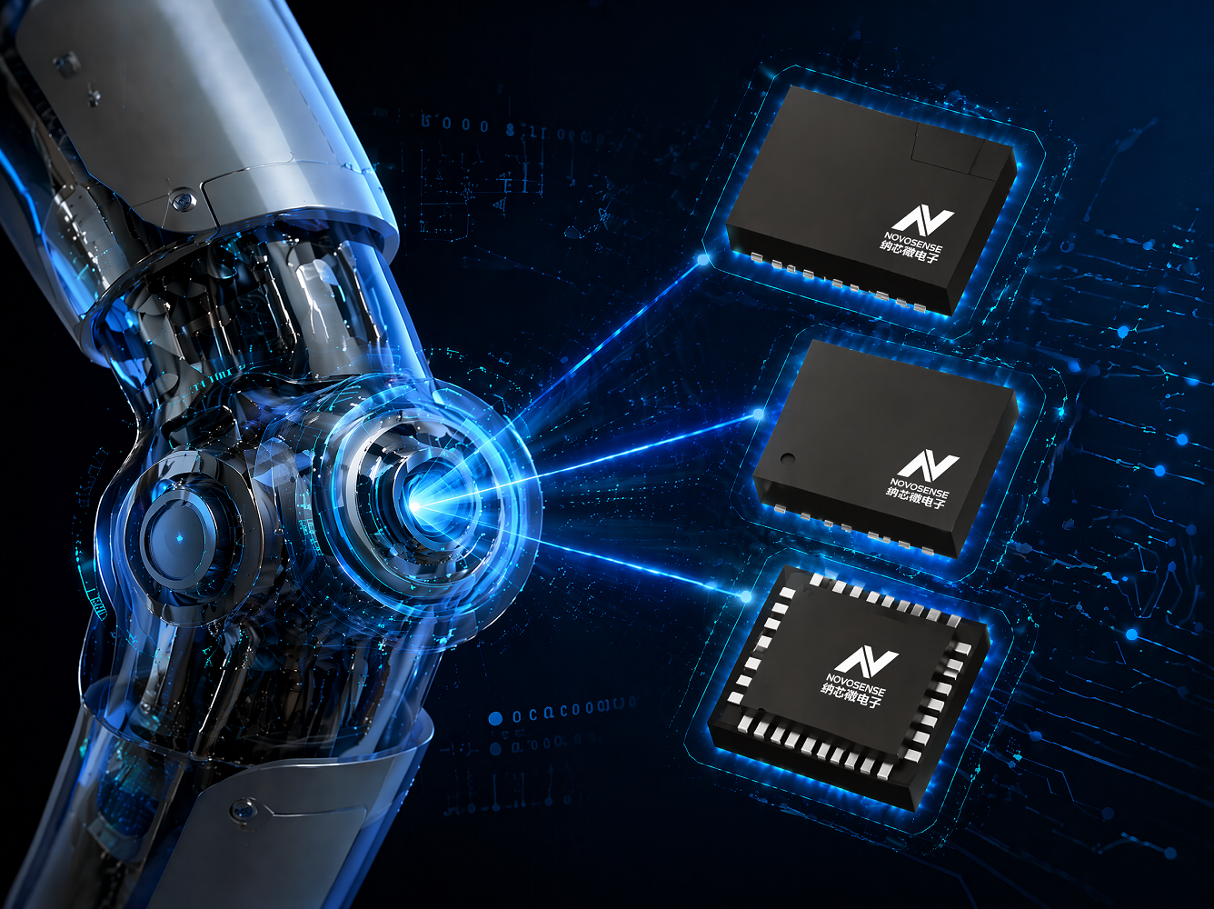
In the previous article,'Humanoid Robots Enter Mass Production: Opportunity Window for Domestic Chips — Sensing Edition,'we discussed the shift in supply-chain economics as humanoid robots move into mass production: the R&D stage seeks rapid validation and no surprises, while mass production requires controllable costs, stable supply, and timely engineering response—these three are precisely natural strengths of domestic chips, providing a natural opportunity window for them. We also broke down the robot joint module, dividing the chip signal chain into three layers—sensing, drive, and power. In the Sensing article, using the domestic encoder solution MagnTek (NOVOSENSE) MT series as an example, we showed the product range from Hall-effect to inductive and from 14-bit to 21-bit; domestic encoders already offer full-scenario coverage for joint-angle feedback, from entry-level to flagship.
The sensing-layer encoder is the first link in the signal chain. It feeds angle information back to the MCU; after the MCU runs the FOC algorithm, it outputs six PWM commands—before these PWM signals reach the MOSFETs, they still need to pass through a gate driver chip. This stage determines whether the MCU's control commands can be accurately and quickly converted into current flowing through the motor windings.This article moves to the second layer of the joint signal chain: the drive layer.

1. Three Drive Architectures: Trade-offs Between Power and Space
The driver layer is not a single product category. Depending on the joint's power level, bus voltage, and space constraints, the driver IC selection logic differs. Overall, it is divided into three architectures.
1. Integrated motor driver SoC.The MCU core, gate pre-driver, and MOSFET full bridge are all packaged in a single chip. With the microcontroller plus power stage, one chip forms a complete small motor drive system. The power ceiling is determined by the package's heat dissipation capability, making it suitable for low-power end effectors such as dexterous hand fingers and expression servos.
2. Isolated half-bridge driver.An electrical isolation barrier is added between the control side and the power side, with withstand voltage up to several thousand volts. When the joint bus voltage is relatively high, or when the overall machine's safety architecture requires isolation between high and low voltage, isolated drive is the baseline configuration. The trade-off is that the physical structure of the isolation barrier increases chip area and adds a small amount of propagation delay.
3. Non-isolated half-bridge driver.The MCU and driver circuit share a common ground, eliminating the size and cost of the isolation stage. One dual-channel chip drives a pair of high-side and low-side MOSFETs; a three-phase joint uses three. The advantage of the non-isolated solution lies in the package—DFN8, DFN10, with a footprint of a few square millimeters—making it suitable for medium-power joints with tight PCB space and moderate bus voltage.
The applicable boundaries of the three architectures are determined by the joint's power level and space constraints. This is almost consistent with the internal tiering logic in the Sensing section—'Hall for cost-effectiveness, AMR for mid-to-high end, inductive for flagship'—except that encoders stratify technical routes within one category (magnetic/inductive angle encoders), whereas the driver layer naturally uses chip architecture as the dividing line.
Which architecture to choose ultimately depends on the specific requirements the joint places on the driver chip.
II. Three Hardware Tests for Driver Chips
The first step in mass-production part selection is whether the hardware specifications can pass muster. The operating conditions of joint motor drives generally have several notable characteristics: high PWM carrier frequency (usually in the 20–50 kHz range), fast motor dynamic response, severe load transients, and dense arrangement of multiple joints with mutual crosstalk. These characteristics pose three hardware tests that gate driver chips must meet.
First: CMTI—common-mode transient immunity, so ground bounce does not cause false triggering.The half-bridge midpoint voltage switches at high speed between 0 V and the bus voltage at tens of kHz. Each switching event superimposes a short-duration but very-high-amplitude common-mode voltage spike on the driver chip's ground line—dv/dt can exceed 100 kV/µs. CMTI measures whether the driver chip can maintain its logic state under such ground-bounce impacts. The consequences of insufficient CMTI are catastrophic: ground bounce flips the internal logic level, a MOSFET that should be off is falsely turned on, the high- and low-side devices conduct simultaneously, the bus is shorted directly to ground, and the joint locks up instantly. In industrial inverter scenarios, the CMTI requirement is usually 50 kV/µs; robot joints have higher PWM frequencies and faster current changes, so in engineering practice, above 100 kV/µs is a common specification for high-end isolated gate driver solutions.
Second: propagation delay—the timing foundation of FOC.From when the MCU pulls the PWM pin high to when the MOSFET gate begins to rise, there is a fixed logic-chain delay inside the driver chip. Taking 20 kHz PWM as an example, half a period is 25 µs—if the propagation delay accounts for 2 µs, it consumes 8% of the effective duty-cycle window. A more subtle problem is the mismatch in propagation delay between the high- and low-side devices (pulse-width distortion): the delay difference directly compresses the effective range of the hardware dead time. If the dead time is set short, delay jitter may cause the high- and low-side devices to briefly overlap and shoot through; if set long, current distortion during the dead time reduces the accuracy of FOC torque control. Low delay and good consistency are the accuracy foundation of the FOC algorithm at the hardware layer.
Third: peak drive current—gate charging/discharging speed.The MOSFET gate is essentially a large capacitor (input capacitance Ciss typically ranges from hundreds of pF to several nF). To drive it from 0 V to 12 V for turn-on, several amperes of current must be injected momentarily. The gate driver's source current determines turn-on speed, while its sink current determines turn-off speed. During switching transitions, the MOSFET simultaneously withstands high voltage and conducts current, producing switching losses. Faster speed means shorter transition time, lower loss, and less heating. Joints have no cooling fan and rely entirely on PCB copper for heat conduction—every watt of switching loss saved adds thermal design margin.
III. NOVOSENSE's Driver Matrix: From Dexterous Hands to Hip Joints
NOVOSENSE is a leading domestic manufacturer in isolation chips and gate drivers—a field long dominated by international giants such as TI and Infineon. As mentioned in the sensing section, NOVOSENSE's acquired Magntek provides an encoder product portfolio ranging from Hall-effect to inductive. At the driver layer, NOVOSENSE's own product line covers three architectures: integrated SoC, non-isolated half-bridge, and isolated half-bridge—encoders and driver chips come from the same supplier, a tangible advantage in BOM management and supply-chain efficiency for complete robot joints.
The following is a selection of models suitable for robot joints.
NSUC1612 Series—the "single-chip joint" for dexterous hands.Taking NSUC1612E as an example, a Cortex-M3 core, three-phase brushless DC motor pre-driver, on-chip MOSFET full bridge, FlexCAN communication interface, and LDO regulator are all integrated in a QFN32 (5×5 mm) package. It has 3 half-bridge outputs, total RDS(on) of about 0.4 Ω, continuous current of 1.4 A, and peak current of 2.1 A. A built-in back-EMF comparator supports sensorless six-step commutation—no Hall sensor is needed for commutation feedback; the motor can self-synchronize based on back-EMF zero crossings, making it suitable for end-effector scenarios that do not require high low-speed torque smoothness. ROM integrates the UDS diagnostic protocol, so in mass production, fault localization and OTA are supported by standardized toolchains; it is AEC-Q100 Grade 1 qualified.
NSUC1602—the SoC driver platform for mainstream joints.It also uses a Cortex-M3 core, but NSUC1602 adopts an external-MOSFET architecture—the pre-driver drives six external N-MOSFETs, raising the power ceiling from 20 W to 1500 W and covering most joints from wrist to hip. It supports FOC vector control and sensored six-step commutation, is AEC-Q100 Grade 0 qualified, and has a full set of SPI and CAN/LIN communication interfaces. Not integrating MOSFETs means the power stage is determined entirely by external MOSFET selection—on the same joint platform, different MOSFETs can cover different torque levels, reducing the driver-side redesign workload for OEMs building multi-model product lines.
NSI6602 Series — Isolated Half-Bridge, the Safety Baseline.CMTI of 150 kV/μs, 5.7 kVRMS reinforced insulation, and 4 A source and 6 A sink peak currents form the baseline for NOVOSENSE isolated half-bridge drivers. Typical propagation delay is 19 ns, with maximum delay matching of 5 ns; this low delay and consistency are leading in the industry. The series is functionally branched by application requirements: the V series (Disable logic) suits mainstream medium-power joints; the N series (Enable logic) provides hardware-level output shutdown when the MCU fails; the M series (built-in Miller clamp) prevents parasitic false turn-on under high dV/dt conditions. Programmable dead time aligns the hardware protection window with the switching characteristics of specific MOSFETs. Suitable for medium-to-large joint part numbers in SOW14 package; three devices form one three-phase half-bridge.
NSD1224 — Compact Non-Isolated Solution.120 V voltage rating, 3 A/-4 A peak drive current, and ultra-small DFN8 and DFN10 packages. Built-in high-side/low-side interlock logic ensures at the hardware level that the MOSFETs on both sides do not receive turn-on signals at the same time. The HS pin is designed to withstand negative voltage, so it will not latch up under negative ground-bounce impacts during inductive-load freewheeling and dead time. When a joint design does not require isolation but needs high-voltage drive capability in a compact space, the NSD1224 provides a lighter-weight option.
By joint scenario:
- Dexterous hand (low-power end effector): NSUC1612E. Fully integrated; a single chip covers MCU, pre-driver, MOSFETs, communications, and power supply.
- Wrist/ankle/forearm (medium power, space constrained): NSD1224. The non-isolated architecture has advantages in PCB area and cost, and the 120 V rating covers common joint bus voltage ranges.
- Elbow/shoulder/hip/knee (main to high-power joints): NSUC1602 plus external MOSFETs (SoC platform solution) or the NSI6602 series (isolated half-bridge solution). Both can drive external high-current MOSFETs; the difference is whether electrical isolation is required between the control side and the power side—hip/knee joints usually have higher bus voltages, so isolation is the safety baseline.
Benchmarked against mainstream international solutions, TI's UCC series and Infineon's EiceDRIVER series have long dominated the isolated gate driver field. The NSI6602 has reached parity with comparable international products on core metrics such as CMTI (150 kV/μs) and propagation delay (19 ns); the NSD1224's HS pin -10 V negative-voltage tolerance design also offers a differentiation advantage among similar non-isolated products. From a mass-production perspective, the cost advantage of domestic solutions in large-scale procurement and the response speed of local technical support are consistent with the logic of the encoder section in the sensing article.
IV. Conclusion
In the joint signal chain, the encoder provides the angle, the MCU runs the FOC algorithm based on it to generate PWM commands, and the gate driver IC amplifies the PWM to a level capable of driving the MOSFETs—the driver layer is an indispensable link between the sensing layer and the power layer. If the driver IC's delay is too large, its CMTI is insufficient, or its drive current cannot drive the gate capacitance, both the upstream encoder accuracy and the downstream MOSFET efficiency will suffer.
From integrated SoCs to isolated half-bridge and non-isolated half-bridge drivers, NOVOSENSE's driver product portfolio can cover the complete chain from dexterous hands to hip joints. Together with the MagnTek MT series encoders from the sensing article, the first two layers of the joint chip chain—sensing and driving—now have corresponding mass-production-ready options within the same supplier system.
That covers the driver layer. But gate driving is only the middle layer of the signal chain—what ultimately converts electrical energy into a magnetic field and makes the motor turn is the six MOSFETs behind it.Next article: Mass production of humanoid robots and the opportunity window for domestic chips—Power Devices.
For more information about NOVOSENSE products or to request samples, please contact: sales@chiplinkstech.com; Mr. Chen, +86 139 2467 5549.

Attachment: Sample Request

WeChat Official Account