
MOSFETs (metal-oxide-semiconductor field-effect transistors) are one of the most fundamental and important devices in electronics. They have electrical performance advantages such as high input impedance, low noise, good thermal stability, and strong radiation resistance, as well as engineering characteristics including small size, light weight, low power consumption, and long life. From consumer electronics (phone chargers, computer motherboards) to industrial control (motor drives, switching power supplies), and further to new energy vehicles and renewable energy systems, MOSFETs run through almost every field of the modern electronics industry, making them the “nerve center of electronic devices” and the cornerstone of the modern electronics industry.
I. Definition and Classification of MOSFETs
(1) What Is a MOSFET
MOSFET—Metal-Oxide-Semiconductor FET; its Chinese name ismetal-oxide-semiconductor field-effect transistor, a voltage-controlled device—a transistor that uses the electric field effect to control current. Composed of metal, oxide, and semiconductor, it conceptually belongs to the insulated-gate field-effect transistor (IGFET) category and is the most commonly used type of field-effect transistor in modern electronic devices. Its core feature is that the electric field effect generated by the gate-source voltage (Vgs) controls the formation and degree of conduction of the conductive channel, thereby regulating the drain-source current (Ids)—no gate current is required (extremely high input impedance) and drive power is minimal, making it an ideal choice for efficient switches and integrated circuits.
We can break down the name MOSFET to understand it better: ① Metal—usually refers to the gate. With the development of semiconductor technology, modern MOSFETs mostly use polysilicon instead of metal as their gate material; ② Oxide—an extremely thin (tens to hundreds of angstroms) insulating oxide layer, usually made of silicon dioxide SiO₂2, which separates the gate from the semiconductor substrate and prevents gate current leakage; ③ Semiconductor (substrate + source/drain)—using silicon (Si) as the base (a few use silicon carbide SiC or gallium nitride GaN); the source (current inlet) and drain (current outlet) are heavily doped regions, and the substrate is a semiconductor of the opposite conductivity type; ④ Field effect—field-effect transistor, abbreviated FET, uses the gate electric field to change the carrier distribution on the substrate surface, forming a “conductive channel” and achieving current control.
(II) What Types of MOSFETs Are There
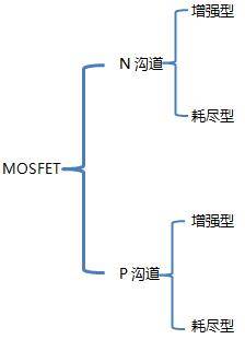
MOSFETs are characterized by an insulating layer between the gate and the channel, so their input resistance is extremely high (up to 10¹⁵ Ω). By internal structure, they can be divided into two types: lateral-structure MOS transistors (conventional type) and VMOS transistors (vertical structure). Generally, however, MOSFETs are mainly divided into two types according to the carrier type in the conductive channel:
①NN-type channel (NMOS):uses electrons as carriers; a positive gate-source voltage (Vgs > 0) must be applied to form a channel; current flows from drain to source; it is the most widely used (e.g., the main switch in switching power supplies);
②PP-type channel (PMOS):uses holes as carriers; a negative gate-source voltage (Vgs < 0) must be applied to form a channel; the current direction is opposite to that of NMOS; it is often paired with NMOS to form CMOS circuits.
Each channel is further divided into the following two types:enhancement and depletion. The so-called enhancement type is normally off; a gate voltage must be applied to form a conductive channel. That is, when VGS (gate-to-source voltage) = 0, there is no conductive channel, and a gate voltage of a certain polarity must be applied (positive for N-channel, negative for P-channel) to form a channel and turn the device on; the depletion type, however, is normally on, and applying a gate voltage reduces or cuts off the conductive channel. That is, when VGS = 0, a channel already exists, and applying a reverse gate voltage can deplete carriers and turn off the channel.

Main market classification chart of MOSFET types
II. Structure and Operating Principle of MOSFET
TakingThe most common N-channel enhancement-mode MOSFETis taken as an example:
(1) Basic Structure
- Substrate: usually P-type silicon, and serves as the device base.
- Source and Drain: two heavily doped N+ regions are formed in the P-type substrate by ion implantation (high carrier concentration, reducing contact resistance).
- Gate: isolated from the substrate by an extremely thin silicon dioxide insulating layer, preventing direct conduction between the gate and the substrate.
- Body/Bulk: connected to the substrate; usually internally shorted to the source (to prevent substrate bias effects from affecting device characteristics).

MOSFET structure schematic (the image is sourced from the Internet)
(II) Operating Principle (using enhancement mode as an example):
① When Vgs = 0 V (gate-source voltage is zero), the MOSFET source and drain are equivalent to two back-to-back diodes, with no conductive path; this is the cutoff state, and D (drain) and S (source) are equivalent to an open circuit, with current Ids = 0.
② When Vgs > Vth (gate-source voltage is greater than the threshold voltage), the positive voltage at the MOSFET gate generates an electric field that, like a magnet, “attracts” negatively charged electrons in the P-type substrate to the surface below the silicon dioxide insulating layer. Therefore, when the voltage (Vgs) is sufficiently large (exceeding the threshold voltage Vth), enough electrons are attracted to form a thin N-type conductive channel on the surface of the P-type substrate. This N-type conductive channel acts like a bridge, connecting the two N+ source and drain regions. At this time, the MOSFET is in the conducting state; if a voltage (Vds) is applied between D and S, current Ids will flow through.
Therefore, a MOSFET can be simply imagined asan intelligent sluice gate precisely controlled by voltage: three key electrodes—Source, Drain, and Gate. The source is the water inlet (current inlet), the drain is the water outlet (current outlet), and the gate is the “handle” that controls the opening and closing of the sluice gate. The threshold voltage (Vth) is the minimum voltage required to drive the “handle”, while the gate voltage (Vgs) is the voltage that drives the “handle”. Taking an N-channel enhancement-mode MOSFET as an example, if the voltage is too low (Vgs < Vth), the gate does not move (the MOSFET is off); conversely, when the voltage driving the “handle” is sufficiently large and Vgs is greater than Vth, the MOSFET turns on, and the larger the voltage, the wider the gate opens and the greater the water flow (the stronger the conduction).
In summary, the core operating principle of a MOSFET is that by applying a voltage (Vgs) between the gate and source that exceeds a specific threshold (Vth), an electric field effect is produced, forming a “conductive channel” in the semiconductor region below the gate that connects the source and drain, thereby allowing current (Ids) to flow. The higher the gate voltage, the “wider” the channel and the larger the current allowed to pass. In other words, applying a voltage to the gate controls the current between the source and drain.
III. Key Parameters
The key parameters are essential for reading a MOSFET datasheet. The following lists several important MOSFET parameters:
| Parameter Symbol | Parameter Name | Parameter Description |
| Vth | Threshold Voltage | The minimum gate-source voltage required to turn on the MOSFET (NMOS: Vth > 0; PMOS: Vth < 0). |
| RDSon | On-Resistance | The DC resistance between the source and drain when the device is fully on (Vgs is sufficiently large). The smaller RDSon is, the lower the conduction loss, the less the device heats, and the higher the efficiency. |
| VDS(max) | Maximum Drain-Source Breakdown Voltage | The maximum reverse voltage that can be withstood between the drain and source, which determines the device's "voltage rating"; exceeding it will cause device damage. |
| Vgs(max) | Maximum Gate-Source Voltage | The maximum voltage that the gate oxide layer can withstand (typically ±20 V). The oxide layer is extremely thin (≈100 Å); overvoltage can easily cause breakdown, so ESD protection must be observed during use. |
| Qg | Gate Charge | The total charge required to charge the gate capacitance to the turn-on voltage. The smaller Qg is, the faster the switching speed (shorter charging time) and the lower the switching loss (P = Qg × Vgs × f), making it suitable for high-frequency applications (such as 1 MHz switching power supplies). |
| ID(max) | Maximum Continuous Drain Current | The maximum drain-source current that the device can safely conduct continuously. |
| Crss | Reverse transfer capacitance | Parasitic capacitance between the gate and drain, affecting high-frequency switching characteristics. The smaller Crss is, the weaker the Miller effect (smaller gate voltage fluctuations), and the higher the switching stability. |
IV. Main Applications of MOSFETs
1. Switching Power Supplies: Because MOSFETs have characteristics such as fast switching speed, low power consumption, and low drive voltage, they can serve as core switching elements and are widely used in switching circuits (such as computer motherboards and mobile phone chargers).
2. Motor Drivers: In H-bridge circuits, they control the forward/reverse rotation and speed of motors (such as in drones, robots, electric vehicles, 3D printers, etc.).
3. Digital Logic Circuits: NMOS and PMOS form CMOS inverters, logic gates, and flip-flops, forming the foundation of all digital chips such as CPUs and memories.
4. Power Amplifiers: They operate in the saturation region (constant-current region) to linearly amplify radio-frequency (RF) or audio signals.
5. Analog Circuits and Power Management: The high input impedance characteristic is used to improve analog circuit performance. For example, in operational amplifiers (input stage), the high input impedance of MOSFETs can reduce signal attenuation and improve circuit accuracy.
V. Product Examples (Using Selected NCE Power Products as Examples)
NCE4060K:The NCE4060K is a trench power MOSFET from NCE Power. It is an N-channel enhancement-mode MOSFET that uses advanced trench technology and design to achieve excellent on-resistance RDS(ON) at low gate charge. Compared with conventional MOSFETs, it offers advantages such as higher cell density, shorter channel length, lower on-state specific resistance, larger conduction current, faster switching speed, and better process compatibility, and can be used in various application scenarios.
| Gate Charge (Qg) | 29nC |
| Threshold Voltage (Vth) | 1.2V~2V |
| Vgs(Max) | ±20V |
| Maximum Continuous Drain Current | 60A |
| On-Resistance | RDS(ON) <7.5mΩ @ VGS=10V
RDS(ON) <15mΩ @ VGS=4.5V |
| Operating Temperature (TJ) | -55℃~+175℃ |
| Transistor Type | N-channel enhancement-mode trench MOSFET (horizontal structure) |
| Power Dissipation (Max) | 65W |
| Reverse Transfer Capacitance Crss | 150pF |
| Drain-Source Voltage (VDS) | 40V |
NCE09N70AT:It is a wide SOA (Safe Operating Area) MOSFET that can meet the requirements of specific circuit applications such as hot swapping, soft start, eFuse, motor drive, and BMS. By optimizing the device structure design and adopting special process technologies, it addresses the challenge of balancing efficiency, thermal management, and reliability in high-power scenarios.
| Gate Charge (Qg) | 128nC |
| Threshold Voltage (Vgs(th)) | 2-4V |
| Gate-Source Breakdown Voltage (Vgs(Max)) | ±20V |
| Drain Current (ID) | 180 A (continuous), 720 A (pulsed) |
| On-Resistance | RDS(ON)<7.5 mΩ@VGS=10V(Typ:6 mΩ) |
| Operating Temperature (TJ) | -55°C to 175°C |
| Transistor Type | N-Channel Enhancement-Mode VMOSFET (Vertical Structure) |
| Power Dissipation (PD) | 474W |
| Reverse Transfer Capacitance (Crss) | 312pF |
| Drain-Source Voltage (VDS) | 70V |
NCEP40P80K:NCEP40P80K is a P-channel enhancement-mode MOSFET utilizing Super Trench technology, which is uniquely optimized to provide the most efficient high-frequency switching performance. Due to the extremely low combination of RDS(ON) and Qg, both conduction and switching power losses are minimized. This device is ideal for high-frequency switching and synchronous rectification.
| Gate Charge (Qg) | 57nC |
| Threshold Voltage (Vgs(th)) | -1.2V~-2.2V |
| Gate-Source Breakdown Voltage (Vgs(Max)) | ±20V |
| Drain Current (ID) | -80A |
| On-Resistance | RDS(ON)=7.2mΩ(typical)@VGS=-10V
RDS(ON)=11mΩ(typical)@VGS=-4.5V |
| Operating Temperature (TJ) | -55℃~175℃ |
| Transistor Type | P-Channel Enhancement-Mode Super Trench MOSFET |
| Power Dissipation (PD) | 150W |
| Reverse Transfer Capacitance (Crss) | 20PF |
| Drain-Source Voltage (VDS) | -40V |
VI. Conclusion: Continuous Evolution Shapes the Future
From basic silicon-based enhancement-mode MOSFETs to advanced silicon carbide devices, MOSFET technology has continued to evolve, with innovation consistently focused on lower conduction losses, faster switching speeds, higher power density, and better thermal performance. As automotive electrification, artificial intelligence, and renewable energy continue to advance, demand for high-performance MOSFETs will only grow, and this fundamental yet critical technology will continue to profoundly shape our future.
Shenzhen Chiplinks Microelectronics Co., Ltd.We can provide a full range of MOSFET samples, technical support, and customized solutions. For further information, please contact: Email: sales@chiplinkstech.com; Tel: 0755-82557621.

Sample request attached

WeChat Official Account