
The lightweighting of new energy vehicles is causing battery packs to shed a natural electromagnetic “iron armor.” To balance energy density and vehicle weight reduction, an increasing number of high-voltage battery pack enclosures are moving from all-steel or all-aluminum structures to multi-material combinations such as steel-aluminum hybrids, high-strength SMC (sheet molding compound) composites, and even carbon-fiber-reinforced plastics. This structural evolution, while delivering weight and cost benefits, also has a side effect: the battery pack’s original natural electromagnetic shielding capability is being weakened.
A closed enclosure made of metal approximates a Faraday cage and can, to a considerable extent, block external radiated interference and contain the escape of internal electromagnetic noise. However, when the enclosure becomes a joined assembly of multiple materials—especially when non-metallic composites are introduced over large areas—the integrity of this “cage” is no longer robust. For the BMS (battery management system) located inside the battery pack, this means the electromagnetic environment it operates in is becoming harsher and harder to predict.
I. Automotive BMS Switching Device Challenges in a Deteriorating Electromagnetic Environment
As the “brain” of the battery system, the BMS contains a large number of switch arrays for high-voltage sampling, as well as switching devices responsible for insulation detection, precharging, balancing, and other functions. These switching elements are like the “nerve endings” of BMS state sensing—when the “nerve signals” are lost in electromagnetic noise, the system’s judgment of key parameters such as cell voltage and insulation resistance may deviate. At a time when 800 V and higher high-voltage platforms are accelerating toward becoming mainstream in the new energy vehicle industry and entering a stage of large-scale adoption, the reliability of these switching devices is directly related to the electrical safety of the vehicle.
In conventional solutions, these switching positions are mainly implemented by mechanical relays and optocoupler relays. Mechanical relays rely on the coil’s magnetic field to pull in an armature and drive contact closure; they have inherent shortcomings such as contact wear, limited operating life, slow response, and a tendency to generate arcs, and they struggle to meet the miniaturization requirements of new energy vehicle battery packs. Optocoupler relays replace mechanical contacts with optocoupling technology and offer improvements in size and speed, but under high-voltage and high-temperature conditions their leakage current is relatively large, which affects the measurement accuracy of insulation impedance; in addition, the LED lumen depreciation effect of optocouplers introduces uncertainty regarding their long-term reliability.
More critically, when the battery pack’s “iron armor” is no longer intact, both types of devices must withstand internal and external electromagnetic interference beyond design expectations under the complex electromagnetic interference conditions in vehicles, causing faults such as false triggering, state jitter, and increased sampling errors, and becoming potential hazards to BMS functional safety. The EMC deficiencies of conventional solutions force engineers to spend considerable effort on board-level remediation, while the root cause lies more in the devices themselves—this is precisely why solid-state relays are highly anticipated by the industry: replacing physical contacts or optocouplers with semiconductor switches improves response speed, operating life, and reliability.
II. NSI7117: A Solid-State Solution Centered on System-Level EMC
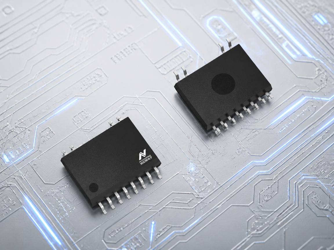
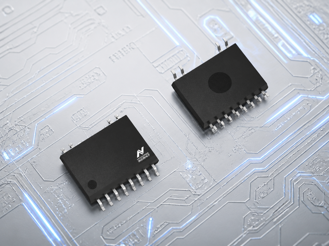
The new-generation NSI7117 series solid-state relays from NOVOSENSE are an integrated solution developed along this technical approach.
Architecturally, the NSI7117 uses NOVOSENSE's mature capacitive isolation technology and integrates two 1700 V SiC MOSFETs, giving the device itself excellent avalanche ruggedness and transient overvoltage withstand capability. When surge spikes occasionally appear on the high-voltage bus, the switch itself will not easily enter an uncontrolled state—this is an important hardware basis for ensuring reliable turn-off of the switch under abnormal operating conditions.

Borrowing the metaphor of “defense and offense,” the EMC design of the NSI7117 can be divided into two lines: “defense” and “offense.”
“Defense” addresses the question of whether the device can be disturbed by the environment to the point of malfunction. In the weakly shielded environment of multi-material battery enclosures, external electromagnetic interference more easily penetrates the enclosure and couples through wiring harnesses into the BMS switch port. Validation data for the NSI7117 show that across the entire test frequency band of the Bulk Current Injection (BCI, ISO 11452-4) test, even when the injection current reaches 200 mA, the device remains at Class A with no functional deviation; the Radiated Immunity (RI, ISO 11452-2) test also reaches Class A; and the simulated handheld transmitter near-field disturbance test (PTI, ISO 11452-9) reaches performance level Class 2 (the standard allows temporary performance degradation during the test). Taken together, these three sets of data provide designers with a clear reference—even in scenarios with SMC enclosures with weaker shielding effectiveness or anisotropic shielding of carbon-fiber enclosures, the logic state of the switch can remain stable and reliable.
“Offense” addresses the question of whether the device itself becomes an interference source. When high-voltage switches turn on and off at tens of kHz or even higher frequencies, they are inherently potential sources of radiated and conducted emissions. If noise caused by switching behavior couples into the sampling chain or communication bus, the measurement noise floor of the entire BMS will rise, affecting insulation detection accuracy in mild cases and triggering system protection in severe cases. The NSI7117's suppression capability in this regard is quantified through a series of tests: Electrostatic Discharge Immunity (ESD, ISO 10605) passes ±8 kV testing in power-off mode; Electrical Fast Transient/Burst (EFT, IEC 61000-4-4) reaches Class 4; and under CISPR 25, conducted and radiated emissions reach up to Class 5. This means lower self-emission characteristics: when the BMS performs system-level EMC validation, the noise component introduced by this switch will be significantly reduced—frequency bands that might otherwise have required additional ferrite beads, common-mode inductors, or even local shielding cans to suppress are now much more manageable from the source.
In addition, the NSI7117's leakage current control under high voltage and high temperature is particularly outstanding: under extreme conditions of 1000 V bias voltage and 125°C, leakage current can be controlled within 1 μA, significantly better than conventional solutions. This provides a clean measurement reference for battery pack insulation detection and can effectively avoid misjudgment of insulation status caused by device leakage current.
Core Electrical Specifications
| Recommended minimum input current | 7mA |
| Input forward/reverse voltage | 2V/6.5V(Max) |
| Output breakdown voltage | >1700V |
| On-resistance (Ron) | 72Ω(25℃);<250Ω(125℃,10mA) |
| Maximum load current | 50mA |
| Leakage current | <1μA(1000V,125℃) |
| Turn-on/turn-off time | <1ms |
| Transient isolation voltage | 5000Vrms |
| Working isolation voltage | 1000Vrms |
| Creepage distance | ≥8 mm between primary and secondary; ≥5.91 mm between switch terminals |
| Operating temperature | -40℃~125℃ |
| Package | SOW12 |
III. Engineering Value and Industrial Significance
If you look at a single solid-state relay in isolation, all it does is replace a pair of contacts or an optocoupler channel; but when it is placed into the complete BMS development chain, you will find that differences in EMC performance are amplified step by step downstream.
As mentioned earlier, in traditional designs, to address the EMC shortcomings of the device itself, engineers must spend a great deal of extra effort—reserving filter networks in the signal chain, repeatedly optimizing routing and ground planes during PCB layout, and urgently adding corrective measures when system-level EMC tests fail. The development time, testing costs, and project risks consumed by these processes usually far exceed the procurement cost of a single device. Leveraging its EMC characteristics that address both emissions and immunity, NSI7117 suppresses noise to an extremely low level right at the device ports, which is equivalent to proactively absorbing the EMC trade-off pressure inside the chip rather than shifting it to the BMS system's board-level design and later-stage remediation. Its significance for shortening development cycles and reducing test rework rates is real engineering value.
Another dimension that should not be overlooked is supply chain and design compatibility. The NSI7117 uses a SOW12 package compatible with mainstream optocoupler relays on the market, which means that when migrating from legacy solutions to solid-state solutions, no major PCB layout changes are required, reducing redesign risk. At the same time, its fully domestic supply chain provides manufacturers with an additional buffer for supply security against the backdrop of remaining localized fluctuations in global chip supply. The automotive-grade version meets the AEC-Q100 Grade1 standard, and its wide operating temperature range of -40°C to 125°C ensures that the device will not become a weak point in system design, whether in extremely cold charging scenarios or high-temperature full-power operation.
From a broader industry perspective, the NSI7117 reflects a directional shift in the competitive dimensions of the entire solid-state relay sector—no longer merely a contest of voltage rating, resistance, and speed, but an upgrade to comprehensive performance competition centered on system-level EMC. This trend applies not only to NEV BMS but also to energy storage system battery cluster management, photovoltaic high-voltage bypass, DC fast-charging power distribution, and industrial high-voltage isolation control. In these fields, switching devices likewise face the dual challenges of complex electromagnetic environments and high reliability requirements. As enclosure shielding characteristics are no longer a fixed variable, system density continues to increase, and functional safety requirements become increasingly stringent, the methodology of designing switching devices with system-level EMC as the anchor is becoming a broader industry consensus.
IV. Limitations and Boundaries
It should be noted that any technical solution has its applicable boundaries. While analyzing the value of the NSI7117, we should also acknowledge the general limitations of the solid-state relay category and the extent to which the NSI7117 addresses these challenges.
Because solid-state relays are based on the inherent characteristics of semiconductor switches, they have a certain on-state voltage drop in the conducting state, which brings additional power loss and heat and requires attention to thermal design in continuous high-current scenarios. In the off state, microamp-level leakage current always exists; it must be controlled at an extremely low level, as in the NSI7117, and calibrated at the system level. In addition, in terms of procurement cost, solid-state solutions are usually more expensive than electromechanical relays of equivalent specifications, but from the perspective of service life and maintenance cost, the total cost over the full life cycle may be more advantageous.
For the NSI7117, its integrated SiC MOSFET is based on a wide-bandgap material, and its on-resistance remains stable throughout the service life, helping to control long-term heat generation. The 50mA load current design focuses its best application scenarios on low-current, high-voltage switching occasions such as high-voltage sampling and insulation detection, rather than on precharge relay positions that need to carry several amperes of inrush current. In these target scenarios, features such as 1700V voltage rating, 1μA leakage current, and system-level EMC optimization can be maximized, while the cost increment accounts for a very small share of the overall BMS BoM. The core problem that the NSI7117 solves is the EMC reliability of switching devices in automotive BMS. It is not a universal switch that is unconditionally superior to all competing products, but a targeted solution that achieves system-level optimization in specific dimensions.
V. Conclusion
What NOVOSENSE offers with the NSI7117 is a technical answer that goes deep on EMC. It does not simply improve parameters on the basis of existing technology; rather, it starts from the actual application scenarios of automotive BMS systems and carries out comprehensive systematic optimization. Future high-voltage switches must not only know how to turn on and turn off, but also understand how to provide stable and reliable safety assurance for the system in a world full of electromagnetic noise.For more information about the NSI7117 or to request samples, please contact the official authorized distributor: sales@chiplinkstech.com; phone: Engineer Chen, 13924675549 (same number on WeChat); WeChat official account: Zhilian Micro - Motor Control Chips, providing part selection services and technical support.

Sample Request Attached

WeChat Official Account