
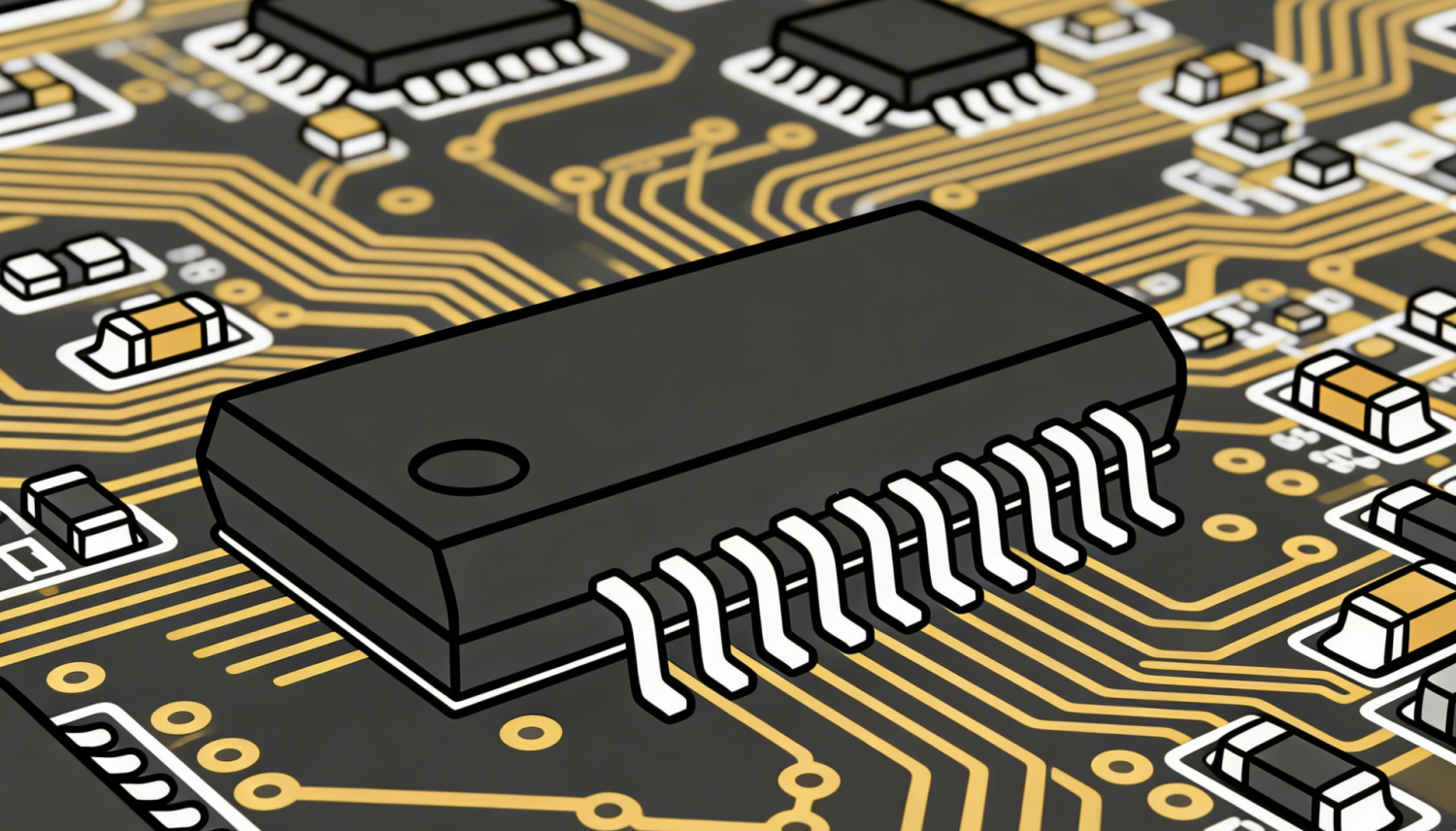
Isolated digital inputs and digital isolators both have “isolated” and “digital” in their names, and both are centered on achieving electrically isolated signal transmission. In practice, however, they are very different. This article explains the core differences between “isolated digital inputs” and “digital isolators,” and also analyzes NOVOSENSE’s industrial-grade isolated digital input chip NSI8608, providing a one-stop, highly integrated solution for isolated signal acquisition designs in industrial automation scenarios.

1. Isolated Digital Inputs ≠ Digital Isolators
An isolated digital input is an integrated device for capturing on/off signals at industrial sites. It provides complete electrical isolation between the field-signal side and the host-controller side, while integrating signal conditioning, level shifting, threshold detection, protection circuits, and other full-chain functions. It is an end-to-end field-signal acquisition solution.
In traditional industrial control (such as PLC) scenarios, when processing 24 V on/off signals from industrial sites, conventional solutions often use one optocoupler plus 7–8 discrete resistors and capacitors to build a single-channel circuit; an 8-channel design requires dozens of peripheral components. This not only takes up a large PCB area but also tends to cause serious heating and a high failure rate. In contrast, isolated digital input chips use a fully integrated architecture to simplify complex discrete circuits, perfectly aligning with the miniaturization, high-density, and high-reliability trends of industrial automation equipment.
Digital isolators generally refer to general-purpose basic semiconductor devices used to achieve electrical isolation between two circuit systems. Their core function is to block direct conduction of DC and low-frequency AC signals through isolation media such as capacitive coupling, magnetic coupling, or optical coupling, while transmitting high-frequency digital logic signals without distortion. They perform only the single function of “isolated transmission” and do not have front-end signal conditioning or level adaptation capabilities.
The core differences between the two are compared below:
| Comparison dimension | Isolated digital input | Digital isolator |
| Core task | A complete end-to-end solution dedicated to industrial field on/off signal acquisition. It directly connects to field switching signals such as buttons and sensors (e.g., 24 V) and transmits them to the MCU after processing. | A device that only performs isolated transmission of digital signals, responsible for digital signal transmission between board-level chips (e.g., MCU and ADC). |
| Input voltage | High voltage (typical 24 V, range 5 V to 60 V), directly addressing industrial field conditions. | Low voltage (typically 3.3 V or 5 V TTL/CMOS logic levels). |
| Power supply method | Only the output side (controller side) needs power; the input side can draw power from the field signal. | Both sides of the isolation barrier require power (VCC1 and VCC2). |
| Integrated functions | Highly integrated with built-in precision current limiting, voltage threshold comparators, etc.; very few external discrete components are required. | Relatively simple functionality, focused on signal isolation and transmission. |
| Typical scenarios | PLC, motor control, and power grid applications, for connecting field-side inputs to host controllers | On-board signal path isolation between ADCs or data acquisition converters and host controllers or microcontrollers |
II. NSI8608: Highly Integrated Isolated Digital Inputs
18-channel + high integration
While understanding the device, selecting the right device is also key. The NSI8608 is an 8-channel highly integrated isolated digital input receiver introduced by NOVOSENSE, featuring IEC 61131-2 Type 1, 2, and 3 characteristics. It integrates all functions required for 8-channel digital inputs—current limiting, signal conditioning, electrical isolation, logic output, and more—into a single SSOP20 package.
For system design, this means: reduced PCB area, enabling I/O modules with smaller size and higher density; fewer BOM items, lowering overall procurement costs; and shorter design cycles, with no need to repeatedly debug the matching of discrete components, reducing R&D and debugging difficulty.

Functional Block Diagram
2Core Technologies and Performance Advantages
From a technical architecture perspective, the input stage of the NSI8608 uses a current-mode input design. It can directly receive wide-range 24 V to 60 V digital input signals and does not require an additional field-side isolated power supply. The input side can draw power directly from the field signal, eliminating one isolated power supply design and simultaneously reducing system cost and design complexity. It uses NOVOSENSE's mature capacitive isolation technology and adaptive OOK modulation technology to transmit digital data through a silicon dioxide isolation barrier: the transmitter represents one digital state with a high-frequency carrier and the other digital state with no carrier, and the receiver completes signal demodulation after advanced signal conditioning. This achieves high-noise-immunity, low-latency signal transmission while also ensuring the long-term service life and reliability of the isolation barrier.
From a functional integration perspective, the NSI8608 includes a built-in full-bridge rectifier (not available in comparable TI products) and current-limiting functionality (not available in comparable SiLabs products). The former enables bidirectional digital input and is natively compatible with both source-type and sink-type input modes without additional hardware switching. The latter provides built-in 2.1 mA (typical) precision current limiting, with power consumption far lower than traditional discrete solutions, significantly reducing system temperature rise and making it suitable for high-density I/O modules.
Key parameters are as follows:
| Feature | Parameter | Description |
| Number of channels | 8 channels | Single-chip processing of multiple signals, high integration |
| Isolation withstand voltage | 3 kVrms (UL1577 certified) | Complies with industrial safety standards |
| Input voltage range | ±60V | Can be directly connected to 24 V industrial field |
| Data transmission rate | DC~2Mbps | Meets high-speed digital signal acquisition requirements |
| Propagation delay | 380ns(tPLH) | Good real-time performance, suitable for applications requiring fast response |
| Integrated current limiting | Typical 2.1 mA | Low power consumption and low temperature rise |
| CMTI (typical) | 75kV/us | Strong common-mode interference immunity |
| Standards compliant | Compliant with IEC 61131-2 Types 1, 2, and 3 | Internationally recognized standard |
| Operating temperature | -40℃~125℃ | Designed for harsh environments |
| Package | SSOP20 | Pinout compatible with mainstream comparable products |
| Safety certifications | UL1577、CQC、CSA、VDE | Complete certifications |
3. Typical Application Implementation (PLC Application Solution)
PLC (programmable logic controller) is the core application scenario for isolated digital input chips. In the design of PLC digital input modules, the NSI8608 demonstrates comprehensive advantages far beyond traditional solutions and comparable competing products:
- No field-side power supply is required; the external circuit needs only one resistor to configure the input-side threshold voltage, making design and calculation easy;
- The integrated rectifier bridge natively supports sourcing and sinking inputs, resulting in a smaller solution size and adapting to the miniaturization trend of PLCs;
- Integrated current limiting reduces overall system power consumption and heat generation;
- It provides a 2 Mbps transmission rate and 380 ns delay; the interface speed is much higher than traditional optocoupler solutions, making it suitable for transmitting high-speed signals such as position feedback in electric drive applications.
Competitor Comparison:
| Comparison Dimensions | NSI8608 | ISO1228(TI) | Si838x(SiLabs) |
| Product Positioning | 8-channel isolated digital input | 8-channel isolated digital input | 8-channel isolated digital input |
| Input voltage range | ±60V | ±60V | ±60V |
| Input type | Bidirectional, native sink/source input support | Bidirectional, hardware-configurable sink/source input switching | Bidirectional, native sink/source input support |
| Field-side power supply | Not required | Required | Not required |
| On-chip integrated current limiting | Built-in 2.1 mA precision current limiting | Resistor-programmable current limiting, requires external resistor configuration | No on-chip integration; relies entirely on an external resistor network |
| Rated isolation withstand voltage | 3kVrms | 3kVrms | 2.5kVrms |
| Data transfer rate | DC~2Mbps | DC~1.5Mbps | DC~2Mbps |
| Propagation delay | 380ns | 780ns | 124ns |
| CMTI | Typical 75 kV/μs | Typical 75 kV/μs | Typical 50 kV/μs |
| Quiescent operating current | Typical at all inputs low: 3.15 mA; typical at all inputs high: 3.5 mA | Logic side typical 3.5 mA, field side typical 3.5 mA (sink mode) | Typical at all inputs low: 4.8 mA; typical at all inputs high: 5.4 mA |
PLCMeasured heat generation of the solution:
Test conditions:At 25°C, with peripheral circuits configured separately per IEC 61131-2 Type 3, a single-channel 30 V DC heat generation test was performed (left figure: Si838x, right figure: NSI8608):

Test conclusion:
- The Si838x has no built-in current-limiting design and relies on external current-limiting resistors for current control. Although the chip itself generated little heat in the test, the temperature of the two external current-limiting resistors reached up to 38°C. Long-term high-temperature operation can easily cause resistor value drift and aging failure, affecting the module's long-term reliability;
- By contrast, the NSI8608 features an integrated current-limiting solution. In testing, the maximum temperature of the chip itself and the peripheral resistors was only about 28°C, outperforming comparable competing products in both overall temperature rise and local hotspot control.
IV. Conclusion
As Industry 4.0 advances in depth, PLCs, motor drives, and grid equipment are all moving toward miniaturization, high density, and high reliability. As the "first gate" for signal transmission, isolated digital inputs—and the choice of solution for them—affect equipment design complexity, hardware cost, and long-term stability.
NOVOSENSE's NSI8608 offers core advantages including 8-channel high integration, ±60V wide adaptability, low power consumption with no field-side power supply required, and high speed with low latency. It has passed multiple safety certifications such as UL1577, CQC, and VDE, fully meeting stringent industrial-grade requirements. It not only solves the pain points of traditional solutions such as complex design, severe heating, and poor reliability, but also offers advantages in performance and cost. Whether for newly designed PLC digital input modules or upgrades of existing legacy products, the NSI8608 enables customers to "spend less money, use less time, and build more stable products." For more information or to request product samples, please contact: sales@chiplinkstech.com (email), Tel: 0755-82557621. Selection services and technical support are provided.

Attached: Sample Request

WeChat Official Account