
Anyone who does motor control has gone through this stage—writing FOC code on the main MCU: Clarke transform, Park transform, current PI, speed closed loop, SVPWM, which takes weeks or even months. Adjusting parameters, tuning response, and tracing waveforms—each step relies on the engineer's accumulated experience.
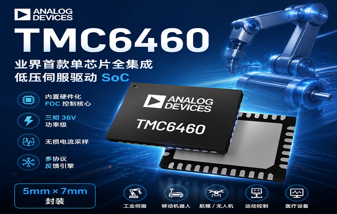
Since 2018, the TMC series, starting with the TMC4671, has been trying one thing: moving FOC from software to hardware. Eight years later, the TMC6460 takes this path to a new level—FOC controller, power stage, current sensing, and feedback engine are all packed into a single 5mm×7mm chip.

1. First, Look at What Traditional Solutions Do
A complete servo drive system, when broken down, typically requires four chips as a foundation:
The first chip: MCU, running the FOC algorithm.Clarke/Park transform, current PI regulation, speed and position closed loop, SVPWM—all executed sequentially by the CPU. However, software FOC has a limitation: its latency is uncertain. The MCU's FOC calculation is usually executed in a timer interrupt, but interrupt response has jitter (depending on what the CPU is doing at the time), and the instruction pipeline also introduces additional cycle fluctuations. Simply put, the actual execution interval of your current loop code is not equal each time—this may not affect most applications, but in high-speed motors and low-inductance motors (phase inductance<0.5mH), microsecond-level delay jitter can distort the current waveform, causing motor heating, reduced efficiency, and increased noise.
Second chip: driver IC or discrete MOSFETs. Converting the PWM signal output by the MCU into power output requires external MOSFETs and gate drive circuitry.
Third chip: current-sense circuit.An external shunt resistor plus an op amp converts phase current into a voltage the MCU can read. The shunt resistor itself dissipates heat (loss is proportional to the square of the current), and it is difficult to guarantee accuracy at both low and high currents—at low currents the signal-to-noise ratio is poor, while at high currents resistor temperature drift affects the reading.
Fourth chip: encoder interface chip.ABN incremental, Hall, SinCos absolute, SPI/SSI—each encoder format may require a different interface circuit. If a project switches from an incremental encoder to an absolute encoder, it is not just the interface chip that must be changed; the PCB layout must be modified as well.
In actual designs, there are also peripheral resistors and capacitors, level shifting, and isolation circuits designed around these chips, further increasing PCB area and BOM cost.
II. TMC6460: Four-in-One
The TMC6460 integrates all four functional modules above into a single 5 mm × 7 mm TQFN38 package. ADI defines it as 'the first servo drive IC to fully integrate an FOC controller, power stage, current sensing, and feedback engine.'
Module 1: Hardware FOC Controller
Inside the TMC6460 there is ahardware module called Motor Control Core (MCC), which implements the complete FOC control chain in hardware logic: Clarke transform → Park transform → current PI (ID/IQ) → decoupling → inverse Park → inverse Clarke → SVPWM.This entire chain executes cycle by cycle in hardware, with a control-loop frequency of up to 200 kHz.
The key lies in 'cycle by cycle.' Running software FOC on an MCU: interrupt arrives → save context → compute Clarke → compute Park → compute PI → compute SVPWM → update PWM duty cycle → restore context → exit interrupt. Although the execution time of each step can be measured, the jitter of those tens of clock cycles in interrupt response cannot be measured accurately; you cannot tell the MCU 'the next interrupt must be serviced exactly 2000 cycles later.'
Hardware FOC is different. Every transform and every PI calculation in the MCC is completed on fixed clock edges. For current sampling → Clarke → Park → PI → inverse Park → inverse Clarke → SVPWM → PWM update, the latency through this loop is fixed and predictable. For low-inductance motors (such as coreless motors, whose phase inductance may be only tens to hundreds of μH), this determinism means the current waveform will not be contaminated by timing jitter.
According to official test data: when running the same load with a Maxon ECXSP08M motor (8 mm diameter, 0.447 mH phase inductance), the TMC6460 achieved a motor temperature 14°C lower than a software FOC solution and saved 8 mA in current consumption. The difference is exactly the efficiency lost to jitter.
The TMC6460's MCC also integrates a8-point ramp generator. It supports up to six independent acceleration/deceleration segments plus one constant-velocity segment, with smooth transitions and minimal jitter. The MCU only needs to send the target position or target velocity; the chip plans the S-shaped acceleration/deceleration trajectory itself. The outer speed PI and position PI controllers are stacked on top of the inner torque PI loop, and the entire control cascade is closed at the hardware level.
Module 2: Three-Phase Power Driver Stage
The chiphas three built-in 36 V half-bridges; the on-resistance of each single FET is 55 mΩ, continuous current is 3 A RMS, and peak current detection supports 5 A (full scale). No external power devices are required. The output slew rate is adjustable in four levels, allowing a trade-off between electromagnetic radiation and drive efficiency.
Module 3: Lossless Current Sensing
The TMC6460 can use the MOSFET's own on-resistance Rds(on) for current sampling; in principle, no external shunt resistor or op-amp is required.
The Rds(on) of a power MOSFET drifts with temperature (positive temperature coefficient), so directly converting current using a fixed ratio introduces error. The TMC6460 does not simply read the voltage drop across Rds(on); it combines an internal high-precision ADC and a dynamic gain amplifier, allowing selection among four equivalent resistance values and four gain settings. Moreover, the gain can be switched in real time during operation: use a low gain setting to protect the range during rapid motor acceleration and current peak surges, and switch to a high gain setting during constant-speed light load to improve small-current accuracy.
This solves a pain point of traditional discrete sensing solutions: if you use a high-power shunt resistor (for example, 50 mΩ), high-current measurement is fine, but at low currents the voltage drop is only a few mV, resulting in very poor SNR. Conversely, with a low-value resistor, low-current accuracy improves, but temperature drift becomes an issue at high currents. Dynamic gain switching uses a hardware approach to cover both operating conditions.
The chip also integrates an automatic Kirchhoff compensation function: when the current of one phase cannot be sampled normally at a high duty cycle, the third-phase current is automatically calculated and reconstructed from the current values of the other two phases, ensuring sampling continuity over the full duty-cycle range.
Module 4: Multi-Protocol Feedback Engine
The TMC6460's feedback engine design is distinctive and highly flexible.
At the hardware level, it natively supports four types of sensor interfaces: digital Hall sensors, ABN incremental encoders, analog Hall sensors, and SinCos sine/cosine encoders. In addition, the feedback engine integrates a speed measurement module and a 32-bit multi-turn position counter, and can simultaneously maintain two independent feedback sources.For example, you can use the ABN incremental encoder on the motor side for the speed loop and current-loop commutation, while using the SSI absolute encoder at the reducer output for load-side position closed-loop control. This is the dual-feedback mode defined in the datasheet and is also a typical requirement for industrial robot joints: motor-side speed measurement ensures dynamic performance, while joint-side absolute position measurement ensures end-point accuracy.
The extension layer is implemented by a built-in programmable I/O controller. SPI/SSI absolute encoders can be driven directly by the ROM firmware of the I/O controller; encoder protocols that are not natively supported, such as BiSS-C and Tamagawa T-format, can also be adapted by uploading a custom decoding program to the I/O controller for execution.The practical value is that when a new project switches to an unfamiliar encoder protocol, there is no need to change chips or redesign the board; adaptation can be completed simply by updating the I/O controller firmware.
In addition, if the host MCU is connected to an external angle sensor, the angle value can be written directly to the TMC6460 through registers, replacing the onboard encoder input.

Simplified application diagram
III. Traditional Solution vs. TMC6460
| Dimension | Traditional Solution | TMC6460 single-chip solution |
| FOC control | MCU runs software algorithms | Hardware FOC core |
| Power driver | External driver IC or MOSFET | Integrated three-phase power stage |
| Current sensing | External shunt resistor + op-amp | Lossless MOSFET on-resistance sensing |
| Encoder interface | External interface chip | Integrated flexible feedback engine |
| Package | Multiple chips combined | Single chip, 5 mm × 7 mm |
There are several effects:
In terms of space,A single 5 mm × 7 mm chip takes over the work previously done by four chips plus peripheral circuitry, reducing the BOM and shrinking PCB area. In scenarios such as crowded wiring inside a robot, one fewer chip saves not only the chip's own area but also a set of power traces, decoupling capacitors, and signal traces—saving system-level space cost.
In terms of development,The FOC algorithm is implemented directly at the hardware layer. Developers no longer need to hand-write hundreds of lines of FOC code, repeatedly tune PI parameters, or trace current waveforms. It can be started by configuring registers through ADI's GUI, greatly reducing the FOC tuning experience required. Although it is not “zero-barrier,” the debugging cycle is significantly shortened.
In terms of performance,The deterministic latency of hardware FOC is the core advantage. The PWM frequency is configurable from 1.83 kHz all the way up to 200 kHz, providing strong adaptability to low-inductance motors.

Pin package diagram
IV. Technical Route Differences of Highly Integrated Solutions
The overall trend in the current motor drive industry is evolution toward high integration. Companies are launching single-chip solutions to simplify peripheral design and shorten development cycles, butthe underlying implementation routes differ from TMC6460's.。
Texas Instruments' MCx series focuses on code-free development, integrating motor-control peripherals with an MCU core; Toshiba's SmartMCD™ series launched in May 2026 also adopts an integrated architecture of an Arm Cortex-M core plus drive circuitry; domestic vendors are following suit, for example, China Micro Semiconductor's CMS32M66xx series, which can reduce peripheral components by more than 30% compared with traditional discrete solutions. These solutions are essentially single-chip integration of "MCU + drive peripherals," with core control logic executed by the CPU.
TMC6460's technical path is different: there is no general-purpose MCU core inside the chip; FOC calculations, ramp generation, current sampling, and encoder decoding are all implemented by dedicated hardware logic. It offloads the real-time computation required for servo drive from the host MCU; the external MCU only needs to perform upper-layer strategy scheduling, target issuing, and status reading, while the determinism and stability of all real-time control are guaranteed by hardware logic.
This all-hardware design approach is also reflected in TMC's other motion control products. TMC5262 for stepper drive also uses an all-hardware implementation of an eight-point controller + StealthChop quiet algorithm; TMC9660 in the higher-voltage range integrates a hardware FOC controller with a gate driver, covering 70V application scenarios; and TMC6460 covers the 36V voltage class, targeting the BLDC/PMSM low-voltage servo market, and is the implementation of this technical route in low-power, high-precision scenarios.
V. Conclusion
The traditional design habit for servo drives is: an MCU runs the algorithm, an external driver IC is used, a sense resistor + op amp perform current sensing, and a separate encoder interface chip handles feedback. This starts with four chips, plus a pile of peripheral components. During debugging, you change one line of code, flash the firmware once, and trace the waveform once.
TMC6460 condenses this flow into one board and a single chip: once the registers are configured, the motor can turn. FOC requires no coding, changing the encoder requires no board redesign, and current sensing incurs no external losses. The specific differences lie in deterministic latency, dynamic precision of current sampling, the programmable architecture of the encoder interface, and the paradigm shift from “the main MCU does all the work” to “the MCU only handles strategy, with all real-time computation offloaded.”
For more information or to request samples, please contact: sales@chiplinkstech.com; Engineer Chen, +86 139 2467 5549.

Sample Request Attached

WeChat Official Account