
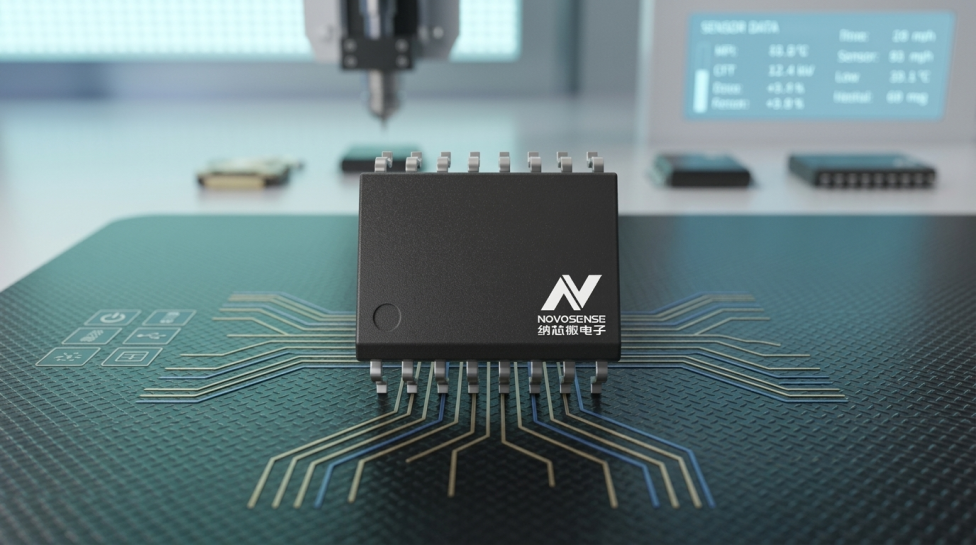
At a time when servo drives and PV inverters are accelerating toward SiC/GaN high-frequency operation, severe voltage transitions caused by power-device switching are becoming a hidden killer of CAN bus bit errors and even lockup. Targeting this industrial-site pain point, NOVOSENSE has officially released a new-generation isolated CAN transceiver—the NSI1150. With a typical common-mode transient immunity of 150 kV/μs, the device builds a robust "firewall" for communication links in high-noise environments. Its pins are also highly compatible with TI's ISO1042 design, providing a more cost-effective and flexible option for localizing industrial communication interfaces.
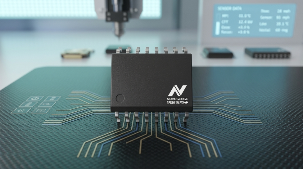
1. Core Performance Analysis: vs ISO1042
The NSI1150 is built on NOVOSENSE's third-generation self-developed capacitive isolation technology, using silicon dioxide as the isolation dielectric and integrating a two-channel digital isolator and a high-reliability CAN transceiver in a single chip. The device is fully compliant with the ISO 11898-2 international standard, supports CAN FD data rates up to 5 Mbps, and covers an operating temperature range of -40°C to 125°C, meeting industrial-grade wide-temperature requirements. Thanks to the highly integrated single-chip solution, the NSI1150 simplifies system design while matching the core performance of the industry benchmark TI ISO1042, with some key metrics achieving industry-leading levels.

Simplified schematic
1. Common-Mode Transient Immunity (CMTI): Industry-Leading
Common-mode transient immunity (CMTI) measures the chip's ability to maintain normal communication when an extremely fast voltage transition occurs across the isolation barrier—the unit kV/μs means the rate of common-mode voltage change in thousands of volts per microsecond that it can withstand, and it is key to determining communication stability on the industrial floor. In applications such as motor drives and frequency converters, insufficient CMTI can cause the receiver to misjudge signal levels, leading to data errors and even bus failure. The NSI1150 has a minimum CMTI of ±100 kV/μs and a typical value as high as 150 kV/μs; compared with the industry benchmark TI ISO1042 (typical ±100 kV/μs, minimum ±85 kV/μs), this achieves an industry-leading level. In strong electromagnetic interference scenarios such as high-speed SiC/GaN switching and motor drives, it reserves greater design margin for communication links and suppresses, at the chip level, the risk of bit errors and bus failure caused by common-mode interference.
2Bus Protection and ESD Immunity: Balancing Robustness and Scenario Adaptability
To address common risks in industrial field buses, such as accidental contact with power lines and ground potential difference fluctuations, the NSI1150 provides ±70 V bus fault protection voltage and a ±30 V common-mode voltage range, consistent with the ISO1042. Even if CANH/CANL are accidentally shorted to the 24 V or 48 V power lines commonly found in industrial sites, the chip will not be damaged immediately—helping reduce on-site maintenance costs and improve equipment robustness.
For ESD protection, the NSI1150 offers an HBM ESD protection rating of ±6 kV on all pins and ±8 kV HBM ESD protection on the CAN bus pins, meeting the application requirements of the vast majority of industrial scenarios. The ISO1042 has the same all-pin ESD protection rating as the NSI1150 and provides ±16 kV HBM ESD tolerance on the bus pins, giving it a certain advantage. However, through an overall hardening design for system-level EFT and surge immunity, the NSI1150 can also provide excellent reliability assurance in real-world applications.
3Isolation Withstand Voltage and Safety Certifications: Flexible Multi-Grade Selection, Full-Scenario Safety Compliance
The NSI1150 offers multiple isolation withstand voltage options. All models have passed the full suite of international safety certifications—UL1577, VDE0884-17, CQC, CSA, and TUV—consistent with the ISO1042 certification system and meeting the entry requirements of mainstream global industrial markets:
- DUB8 and SOP8 packages support 3 kVrms isolation withstand voltage and 7 kV isolation barrier surge withstand; the DUB8 has a minimum creepage distance/clearance of 6.5 mm, suitable for general industrial scenarios with basic isolation;
- SOW8 and SOW16 packages support 5 kVrms isolation withstand voltage and 10 kV isolation barrier surge withstand, with a minimum creepage distance/clearance of 8 mm, suitable for high-voltage scenarios requiring reinforced isolation;
- The SOWW8 package supports 7.5 kVrms isolation withstand voltage and 12.8 kV surge withstand, with a creepage distance of 15 mm, suitable for demanding application requirements.
ISO1042, on the other hand, provides a fixed 5 kVrms isolation withstand voltage, and specific reinforced models support 10 kV surge tolerance. The multiple isolation specifications of the NSI1150 allow engineers to flexibly select models according to the safety requirements and cost constraints of the specific system, avoiding overdesign.

NSI1150 Selection Table
4Power Supply Compatibility and Timing Performance: Compatible with Mainstream Designs
On power supply compatibility. The controller-side supply VDD1 of the NSI1150 supports 2.5 V to 5.5 V, enabling seamless interfacing with MCUs using 2.5 V, 3.3 V, and 5 V logic levels; the bus-side VDD2 is 4.5 V to 5.5 V. The lower limit of VCC1 for TI's ISO1042 is 1.71 V, allowing direct connection to 1.8 V low-power MCUs; in this respect, the ISO1042 offers broader adaptability. However, for industrial control scenarios where 3.3 V and 5 V are the mainstream logic levels, the NSI1150's supply range is sufficient to cover the vast majority of requirements.
In terms of timing performance, both fully meet the timing requirements of 5 Mbps CAN FD: the NSI1150 has typical loop delays of 149 ns (recessive→dominant) and 148 ns (dominant→recessive), with a maximum delay of 210 ns; the ISO1042 has typical delays of 122 ns (recessive→dominant) and 152 ns (dominant→recessive), with maximum delays of 192 ns and 215 ns, respectively. In practical application systems, the performance difference between the two is almost negligible.
More notably, the SOP8 package of the NSI1150 is fully compatible with the SOIC8 package pin hardware pads of TI's ISO1042. This means the two have the hardware basis for board-level pin-to-pin compatibility, reducing the technical threshold and validation cost of supply chain diversification.
Main Parameter Comparison Table
| Parameter | NSI1150 | ISO1042 |
| CAN FD maximum data rate | 5Mbps | 5Mbps |
| CMTI | 150kV/μs | 100kV/μs |
| Bus protection withstand voltage | ±70V | ±70V |
| Isolation voltage | 3k/5k/7.5kVrms | Fixed 5 kVrms |
| Isolation barrier surge withstand | 7kV/10kV/12.8kV | 6 kV (basic) / 10 kV (reinforced) |
| HBM ESD on all pins | ±6kV | ±6kV |
| Electrical clearance | 15 mm (SOWW8 package) | 8.5 mm (SOIC8 package) |
| Maximum loop delay | 210ns | 195ns/215ns |
| Controller-side supply range | 2.5V~5.5V | 1.71V~5.5V |
| Operating temperature | -40℃~125℃ | -40℃~125℃ |
II. Comprehensive Hardware Protection Mechanisms
In terms of protection capability, the NSI1150 matches the ISO1042 and includes comprehensive built-in hardware protection mechanisms:
- TXD dominant-state timeout function: When the TXD pin is continuously pulled low due to an MCU software crash or hardware fault, the NSI1150's internal timer (typical value 2.5 ms, minimum 1.2 ms, maximum 4 ms) automatically disables the transmitter and releases the bus back to the recessive state. This function prevents a single-node fault from "hijacking" the entire bus, ensuring that normal communication of other nodes is not blocked.
- Overcurrent protection: When CANH or CANL is accidentally shorted to a power rail, the current-limiting circuit in the output stage intervenes immediately. The short-circuit output current IOS(D) is limited to -105 mA when CANH = 30 V and to 105 mA when CANL = 30 V. This protection mechanism buys time for system troubleshooting and prevents permanent damage to the output driver due to overcurrent.
- Overtemperature protection: The chip's thermal shutdown threshold TTS is typically 170°C. When the chip junction temperature exceeds this threshold, the output driver is disabled and is re-enabled only after the temperature falls and TXD returns to the recessive state. This design specifically accounts for high-temperature industrial environments, ensuring that the chip does not fail due to overheating under extreme operating conditions.
- Full-chain supply undervoltage lockout (UVLO): When the supply voltage is abnormal, the undervoltage lockout circuit triggers protection in a timely manner, preventing the chip from malfunctioning under abnormal supply conditions.
- Unpowered high-impedance bus: When the chip is unpowered, the CANH/CANL pins are in a high-impedance state and do not interfere with the bus network.
These features are fully aligned with the core protection mechanisms of the TI ISO1042, building a defense system at the chip level against common failure modes in industrial environments and ensuring long-term stable system operation.
III. Application Scenarios
With industry-leading performance, the NSI1150 can be widely adapted to many core industrial and new energy scenarios:
- Industrial inverters and servo drives: In motor drive applications, high dv/dt transients and strong electromagnetic interference generated by high-power inverters are the main threats to CAN communication. With a typical CMTI of 150 kV/μs, the NSI1150 provides sufficient immunity protection for the communication link, reducing bit errors and retransmissions caused by common-mode interference at the source and ensuring the real-time control accuracy and stability of the drive system.
- PV Inverters and Energy Storage Systems: In PV systems with multiple strings operating in parallel, the DC-side voltage can reach up to 1500 V, and the systems must also withstand extreme outdoor environmental effects such as lightning strikes and surges. The NSI1150 provides 5 kVrms isolation withstand voltage and 10 kV/12.8 kV surge withstand capability; its wide-body package meets safety requirements for high creepage distance, making it suitable for communication designs in PV inverters and energy storage BMS under standards such as IEC 62109.
- Communications and Server Power Supplies: In AI server power management systems, multi-module parallel architectures require real-time monitoring of voltage, current, and temperature status, and the CAN bus carries a large volume of diagnostic data traffic. The NSI1150 supports 5 Mbps CAN FD high-speed communication and combines high isolation withstand voltage with low loop delay, providing physical-layer support for reliable communication between high-voltage power modules and low-voltage control circuits.
IV. Conclusion
Grounded in its mature in-house capacitive isolation technology, NOVOSENSE has built a full ecosystem product portfolio that includes isolated drivers, isolated sampling, isolated interfaces, isolated power supplies, and digital isolators. The launch of the NSI1150 further improves its product layout in the industrial communication interface field and is an important practice of the “Isolation+” concept.
Its “Isolation+” concept not only builds safety boundaries for systems through multi-level insulation products, but also enables collaboration across all product categories based on core isolation IP, deeply empowering high-voltage, highly integrated industrial and new energy application scenarios. As a result, NOVOSENSE can provide one-stop, highly reliable chip solutions—from signal sampling and power driving to communication interfaces—for core applications such as electric vehicles, PV-storage-charging, and server power supplies.For more information about the NSI1150 or to request samples, please contact the official authorized distributor:
- Email: sales@chiplinkstech.com;
- Phone: Engineer Chen, 13924675549 (same number on WeChat);
- Official website: https://www.chiplinkstech.com/.
Provides product selection services and technical support.

Sample application attached

WeChat Official Account