
In the first article“Sensing Edition”, we established a macro framework for the shift in supply-chain cost-accounting logic during the mass-production breakout—from “get functionality working first” in R&D to controllable cost, stable supply, and timely response—and broke down the three-layer structure of the joint-chip signal chain, introducing MagnTek (NOVOSENSE) encoder products, which have full-scenario coverage capability in joint angle feedback.The “Drive Edition”then immediately filled in the second layer of the signal chain—three architectures from integrated SoC to isolated/non-isolated half-bridge—and verified that NOVOSENSE has no domestic-adaptation shortcomings in the three hardware tests: CMTI, propagation delay, and drive current.
With these two articles done, one final link remains in the signal chain: the encoder provides angle and the driver chip amplifies PWM, but these control signals must ultimately become real current flowing through the motor windings—this step is handled by the power layer. This article moves into the third layer of the joint signal chain: the Power Edition.
The power stage of a three-phase brushless DC motor joint consists of six power devices forming a full bridge—the high-side arm connects the bus voltage to the motor phase lines, and the low-side arm provides the current return path. Joint torque, efficiency, and heat generation are jointly determined by these six devices' on-resistance, switching speed, thermal resistance, and other factors. For medium- and large-sized joints using discrete power devices, a humanoid robot uses six per joint; with more than thirty joints, that is nearly two hundred devices—the power stage is the highest-volume and most heat-concentrated part of the entire signal chain.

1. Mainstream Industry Choice: Silicon MOSFETs
Current mainstream humanoid robot platforms have bus voltages between 48 V and 100 V; phase currents vary widely by joint type: fingertip grippers in end effectors are usually within a few amperes, while hip and knee joints can reach tens of amperes. Within this voltage and current window, silicon-based MOSFETs, with their mature product ladder, controllable cost structure, and long-term engineering practice, are the current mainstream choice in the industry.
Among silicon MOSFETs, Trench MOSFETs and shielded-gate MOSFETs (Shielded Gate Trench, SGT) are the two major technology platforms primarily suited to robot joints. Their structural differences are significant, and the selection logic therefore diverges.
- Trench MOSFET: Trench-Gate StructureIt has been the main line of low-voltage MOSFET process evolution over the past two decades—replacing the traditional planar gate with a vertical channel to achieve lower on-resistance at the same die area. The process is mature, cost is low, and the supply ecosystem is complete. In low-current scenarios, conduction loss itself is relatively low (I²R), so the Trench platform's cost-performance advantage is more pronounced.
- Shielded-Gate MOSFET (SGT).A field plate is inserted into the trench to form charge coupling, structurally breaking the conventional silicon MOSFET trade-off in which lower on-resistance means higher gate charge—RDS(on) and Qg can be optimized simultaneously. Platform vendors use different generational names for their SGTs (e.g., Infineon OptiMOS, onsemi PowerTrench, NCE Power SGT-III), but the structural principle is the same. In scenarios where high-current turn-off loss trades off against conduction loss, SGT is the optimal silicon MOSFET solution in terms of efficiency.
If the complete system adopts a high-voltage bus scheme above 150 V, medium- and high-voltage superjunction MOSFETs will enter the selection scope. However, the bus voltages of current mainstream humanoid robot platforms are all in the 48–100 V range, so low-voltage Trench and low-to-medium-voltage SGT are the main battleground for joint power devices.
II. Three Facets of Power: Conduction, Switching, and Heat Dissipation
The selection logic for power devices differs from that of the previous two layers. Encoders pursue angular resolution and latency, gate drivers pursue signal integrity, and power devices have only one core proposition: efficiency. All selection dimensions—on-resistance, switching speed, and package thermal resistance—are essentially different facets of efficiency.
- On-Resistance—Every milliohm counts. When a joint is at full load, the conduction loss of each MOSFET is I² × RDS(on). For a finger joint with 3 A current and 25 mΩ on-resistance, the conduction loss is about 0.2 W—almost no heat. For a knee joint with 70 A current and 2 mΩ on-resistance, the conduction loss is nearly 10 W—six devices together total tens of watts, mainly relying on PCB copper for heat conduction. The magnitude relationship here is easily overlooked: light-load joints have far greater tolerance for RDS(on) than intuition suggests—the magnitude of I² naturally keeps the product at a very low level. Once the phase current enters the tens-of-amperes range, every 1 mΩ difference in RDS(on) is amplified by I² into several watts of additional heat dissipation. The interior of the joint mainly relies on PCB copper and the metal housing for passive cooling, so every watt is design margin.
- Switching Speed—The linkage point between the driver layer and the power layer. The peak drive current of the gate driver IC determines the MOSFET gate charging speed, but the total gate charge Qg itself is determined by the MOSFET. In joints with 20 kHz PWM, if the switching transition time is kept within 50 ns, the transition loss accounts for a very low proportion of the switching period. However, high-current MOSFETs naturally have relatively high Qg (tens to hundreds of nC), and if the transition time is stretched to hundreds of nanoseconds, the switching loss proportion rises significantly. This means gate driver IC selection and MOSFET selection need to be coordinated.
- Package——The thermal ceiling. There is no active air cooling inside the joint; heat dissipation relies mainly on PCB copper and the metal housing for passive cooling. The thermal resistance (θJA) of the MOSFET package directly determines how high the junction temperature can rise at a given power dissipation. The typical thermal resistance of a DFN5×6 package is on the order of 40 to 50°C/W—at 2W power dissipation, this means the junction temperature is 80 to 100°C above ambient; at a 40°C ambient, the junction temperature is already close to the upper limit. High-power joints must use larger packages or multiple devices in parallel to spread the per-device power dissipation. Paralleling multiple devices introduces current-sharing requirements—the positive temperature coefficient of MOSFET RDS(on) helps thermal balancing, but differences in layout parasitic inductance can cause uneven dynamic current distribution during switching.
Selecting the power layer for a joint is essentially an iteration among three dimensions: RDS(on), Qg, and package thermal resistance—lower RDS(on) a little, then check how much Qg has increased; determine whether the package's heat-dissipation capability can handle the resulting increase in switching loss; then look back to see whether the gate-drive current is sufficient to drive this gate capacitance. This is not a matter of picking a single optimal value from a datasheet, but a multi-constraint optimization loop.
Once entering mass production, the constraints on this optimization loop are tightened further—mass-production consistency requirements reduce allowable dispersion: batch-to-batch RDS(on) drift, Qg distribution width, and individual differences in package thermal resistance all require engineering margin to be reserved during the selection stage. In the prototype stage, the number of devices is small and batches are concentrated, so parameter dispersion is not easily exposed; mass production faces a cross-batch, large-scale consistency test—the more sufficient the margin reserved during selection, the higher the mass-production first-pass yield.
III. From DFN2×2 to DFN5×6: NCE Power's Joint MOSFETs
The starting point for selecting joint power devices centers mainly on the PCB's physical space and heat dissipation.
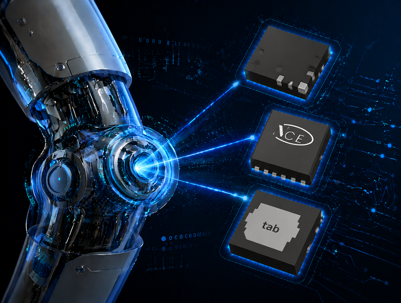
From dexterous hands to hip joints, joint volumes differ by dozens of times, and the corresponding MOSFET packages span from DFN 2×2 to DFN 5×6—NCE Power's two major platforms, Trench and SGT-III, each occupy key positions along this package-size line. The following uses specific part numbers as examples:
- NCE6010J——The entry-level choice for finger grippers. Trench platform, 60V voltage rating, DFN2×2 package—about 4 mm² in area, which is an extremely small package among power MOSFETs. ID 10A (rated), RDS(on) typical value 24.5 mΩ, Qg 25.3 nC. The phase current of finger grippers and facial-expression servos is usually in the 2A to 5A range. Calculated at 3A: conduction loss is about 0.22W, and switching loss is on the order of milliwatts—less than 0.25W total, which leaves ample thermal margin for a device with PD=3W. The core value of this chip is that, with its extremely small 4 mm² package and competitive BOM cost, it fits a complete half-bridge arm into an end effector with severely limited space.
- NCEP046NH80QW——The efficiency upgrade for wrists and ankles. SGT-III platform, 80V voltage rating, DFN3.3×3.3 package. ID 118A, RDS(on) typical value 4.0 mΩ, Qg 30.5 nC. The phase current of wrist and ankle joints is in the 10A to 20A range. Calculated at 15A: conduction loss is about 0.9W, and switching loss is likewise on the milliwatt level—about 1W total. The significance of this part number is that SGT-III's shielded-gate structure enables it to achieve 4 mΩ in a 3.3×3.3 package—at the same package size, its on-resistance is significantly lower than that of traditional Trench products, and it begins to deliver real efficiency gains in medium- and high-current joints. The 80V voltage rating provides ample safety margin for a 48V bus.
- NCEP033NH80GU——The workhorse for elbow, shoulder, and hip joints. SGT-III platform, 80 V rating, DFN 5×6 package. ID 165 A, RDS(on) typ. 3.0 mΩ, Qg 47.4 nC. Phase currents for elbow, shoulder, and hip joints range from 30 to 50 A; at a 40 A operating condition: conduction loss is about 4.8 W, and switching loss accounts for a very low share. The 3 mΩ resistance really delivers at the tens-of-amps level—at 40 A, increasing the resistance from 3 mΩ to 5 mΩ adds 3.2 W of conduction loss per device, and six devices add up to nearly 20 W. For a confined joint cavity, this few-watt difference directly determines whether the thermal design exceeds the heat-conduction limit of the PCB copper. Qg 47.4 nC is within the coverage of the NSI6602 series in the gate driver section (6 A/-8 A peak drive current).
- NCEP021NH80GU——The heavy-load choice for knee joints. SGT-III platform, 80 V rating, DFN 5×6 package. ID 244 A, RDS(on) typ. 1.9 mΩ, Qg 80 nC. Knee joint phase current can reach 60 to 80 A; at a 70 A operating condition: conduction loss per device is about 9.3 W, and total loss for six devices is about 56 W. 1.9 mΩ is one of the best RDS(on) typical values in the 80 V class of DFN 5×6 packages. Qg 80 nC requires the driver chip to provide at least 4 A-level peak source current—the 6 A source current of the NSI6602 series in the gate driver section just covers it. Within the thermal boundary of a single device, paralleling multiple devices can further reduce the equivalent on-resistance and per-device power dissipation, but current sharing considering parasitic inductance in the layout must be designed concurrently.
NCE Power Low-Voltage MOSFETs from the Perspective of Joint Scenarios
| Scenario | Part Number | Technology Platform | Voltage Rating | Package | RDS(on) typ | Qg |
| Finger | NCE6010J | Trench | 60V | DFN2×2 | 24.5mΩ | 25.3nC |
| Wrist/Ankle | NCEP046NH80QW | SGT-III | 80V | DFN3.3×3.3 | 4.0mΩ | 30.5nC |
| Elbow/Shoulder/Hip | NCEP033NH80GU | SGT-III | 80V | DFN5×6 | 3.0mΩ | 47.4nC |
| Knee | NCEP021NH80GU | SGT-III | 80V | DFN5×6 | 1.9mΩ | 80nC |
IV. Conclusion
Sensing layer, driver layer, and power layer—the three articles together break down a complete signal chain for humanoid robot joint chips.
The sensing article demonstrated that the opportunity window for domestic chips during the mass-production boom is real, and provided the first layer of empirical evidence with MagnTek's MT series encoder matrix, ranging from 14-bit Hall-effect to 21-bit inductive encoders. The driver article presented NOVOSENSE's full-architecture drive solutions, from integrated SoCs to isolated/non-isolated half-bridge drivers, proving that the driver layer has no domestic-adaptation shortfall in the three hardware metrics of CMTI, propagation delay, and drive current. The power article presented NCE Power's power-device ladder from Trench to SGT-III—from DFN2×2 for finger grippers to DFN5×6 for hip/knee joints; for each tier of joint power demand, products with the corresponding voltage rating and on-resistance are available.
The encoder provides angle, the gate driver amplifies PWM, and the power device converts electrical energy into a magnetic field—the three chip layers close sequentially along the signal chain. When complete-machine manufacturers move from R&D validation with dozens of prototypes to thousand-unit-level mass-production ramp-up, and selection criteria switch from “functions working” to “predictable supply system,” each of the three domestic chip layers corresponds to suppliers with mass-production delivery capability, forming a complete solution that can enter BOM evaluation.
For more information about NCE Power MOSFET products or to request samples, please contact: sales@chiplinkstech.com; Mr. Chen, 13924675549.

Sample request attached

WeChat Official Account